CGY81 データシートの表示(PDF) - Siemens AG
部品番号
コンポーネント説明
メーカー
CGY81 Datasheet PDF : 12 Pages
| |||
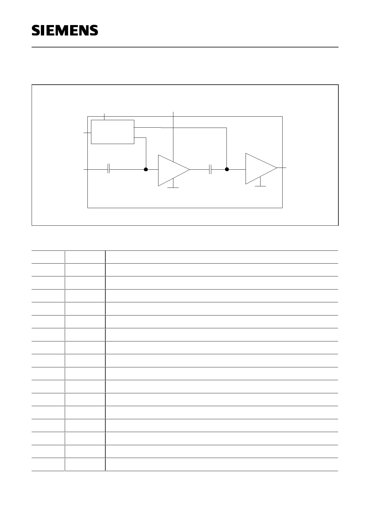
Functional Block Diagram:
Vneg
VD1
Vcon
Control
Circuit
RF IN
CGY 81
RF OUT
Pin Configuration:
Pin #
1
2
3
4
5
6
7
8
9
10
11
12
13
14
15
16
Name Configuration
VD Cell Drain voltage preamplifier stage
n. c.
RF IN Cell RF IN
n. c.
Vneg Negative voltage
Vcon Control voltage
n. c.
n. c.
n. c.
n. c.
RF out RF out / drain voltage final stage
RF out RF out / drain voltage final stage
RF out RF out / drain voltage final stage
RF out RF out / drain voltage final stage
n. c.
n. c.
Siemens Aktiengesellschaft
2
Semiconductor Group
2
23.07.98
HL HF PE 1G9a9A8s-111/-F0o1
Share Link: 