CS5203A-1 データシートの表示(PDF) - ON Semiconductor
部品番号
コンポーネント説明
メーカー
CS5203A-1 Datasheet PDF : 10 Pages
| |||
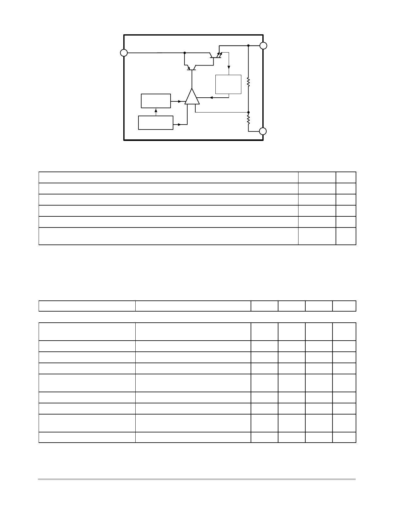
CS5203A−1, CS5203A−2, CS5203A−3, CS5203A−5
VOUT
VIN
Thermal
Shutdown
Bandgap
Output
Current
Limit
− + Error
Amplifier
GND
Figure 2. Block Diagram − CS5203A−2, −3, −5
MAXIMUM RATINGS
Parameter
Value
Unit
Supply Voltage, VCC
Operating Temperature Range
17
V
−40 to +70
°C
Junction Temperature
150
°C
Storage Temperature Range
−60 to +150 °C
Lead Temperature Soldering:
Wave Solder (through hole styles only) (Note 1)
Reflow (SMD styles only) (Note 2)
260 Peak
230 Peak
°C
Maximum ratings are those values beyond which device damage can occur. Maximum ratings applied to the device are individual stress limit
values (not normal operating conditions) and are not valid simultaneously. If these limits are exceeded, device functional operation is not implied,
damage may occur and reliability may be affected.
1. 10 second maximum.
2. 60 second maximum above 183°C.
ELECTRICAL CHARACTERISTICS (CIN = 10 mF, COUT = 22 mF Tantalum, VIN − VOUT = 3.0 V, VIN ≤ 15 V,
0°C ≤ TA ≤ 70°C, TJ ≤ +150°C, unless otherwise specified, Ifull load = 3.0 A.)
Characteristic
Test Conditions
Min
Typ
Max
Unit
Adjustable Output Voltage (CS5203A−1)
Reference Voltage (Notes 3 and 4)
Line Regulation
Load Regulation (Notes 3 and 4)
Dropout Voltage (Note 5)
Current Limit
VIN − VOUT = 1.5 V; VAdj = 0 V,
10 mA ≤ IOUT ≤ 3.0 A
1.5 V ≤ VIN − VOUT ≤ 6.0 V; IOUT = 10 mA
VIN − VOUT = 1.5 V; 10 mA ≤ IOUT ≤ 3.0 A
IOUT = 3.0 A
VIN − VOUT = 3.0 V; TJ ≥ 25°C
VIN − VOUT = 15 V
1.241
1.254
1.266
V
(−1%)
(+1%)
−
0.04
0.20
%
−
0.03
0.4
%
−
1.05
1.15
V
3.2
5.5
−
A
−
2.5
−
A
Minimum Load Current
Adjust Pin Current
VIN − VOUT = 7.0 V
−
−
1.2
6.0
mA
−
50
100
mA
Adjust Pin Current Change
1.5 V ≤ VIN − VOUT ≤ 4.0 V;
10 mA ≤ IOUT ≤ 3.0 A
−
0.2
5.0
mA
Thermal Regulation
30 ms pulse; TA = 25°C
−
0.003
−
%/W
3. Load regulation and output voltage are measured at a constant junction temperature by low duty cycle pulse testing. Changes in output
voltage due to thermal gradients or temperature changes must be taken into account separately.
4. Specifications apply for an external Kelvin sense connection at a point on the output pin 1/4” from the bottom of the package.
5. Dropout voltage is a measurement of the minimum input/output differential at full load.
http://onsemi.com
2
Share Link: 