CS5203A-1 データシートの表示(PDF) - ON Semiconductor
部品番号
コンポーネント説明
メーカー
CS5203A-1 Datasheet PDF : 10 Pages
| |||
CS5203A−1, CS5203A−2, CS5203A−3, CS5203A−5
The ESR of the output capacitor causes an immediate drop
in output voltage given by:
DV + DI ESR
For microprocessor applications it is customary to use an
output capacitor network consisting of several tantalum and
ceramic capacitors in parallel. This reduces the overall ESR
and reduces the instantaneous output voltage drop under
load transient conditions. The output capacitor network
should be as close as possible to the load for the best results.
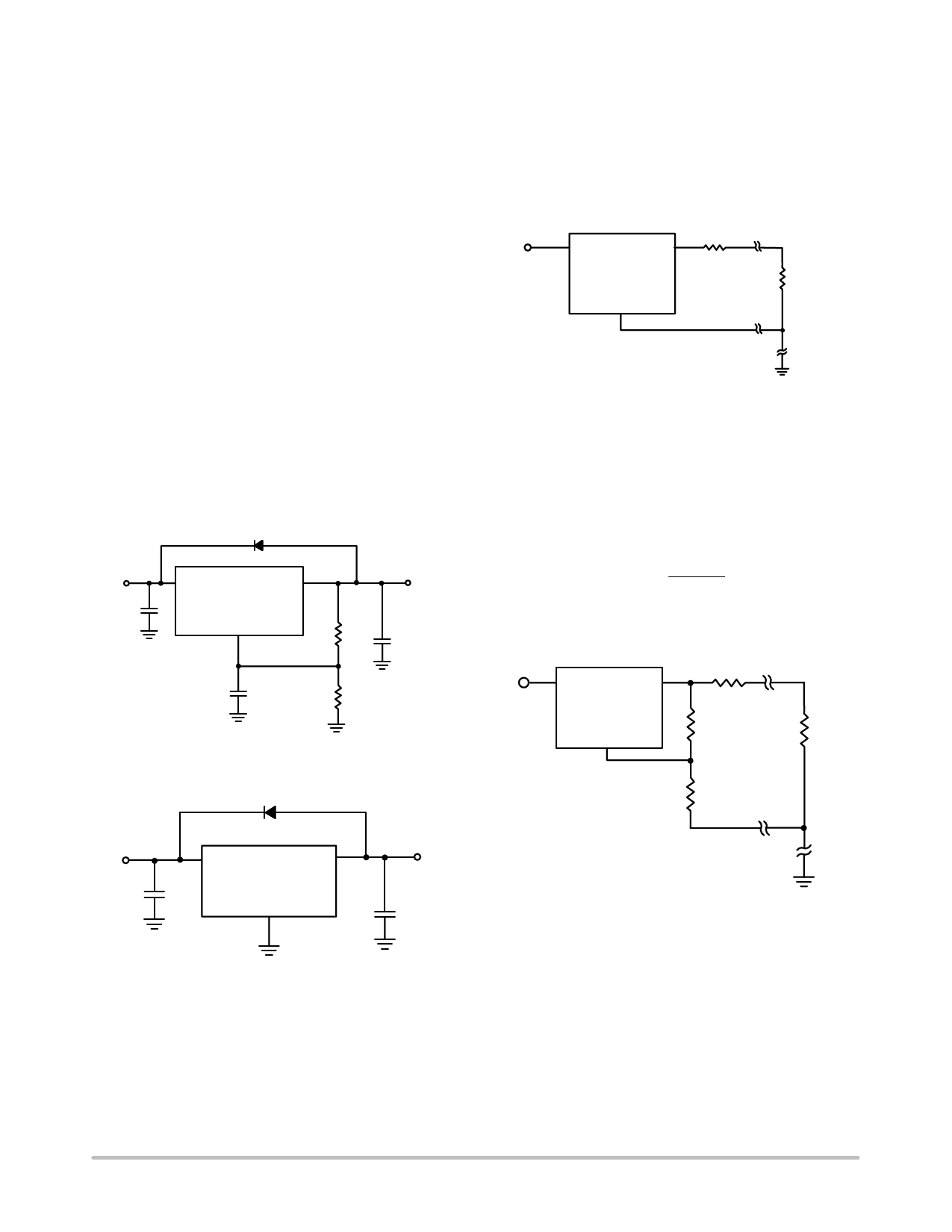
Protection Diodes
When large external capacitors are used with a linear
regulator it is sometimes necessary to add protection diodes.
If the input voltage of the regulator gets shorted, the output
capacitor will discharge into the output of the regulator. The
discharge current depends on the value of the capacitor, the
output voltage and the rate at which VIN drops. In the
CS5203A−X family of linear regulators, the discharge path
is through a large junction and protection diodes are not
usually needed. If the regulator is used with large values of
output capacitance and the input voltage is instantaneously
shorted to ground, damage can occur. In this case, a diode
connected as shown in Figures 11 and 12 is recommended.
VIN
C1
IN4002 (optional)
VIN
VOUT
CS5203A−1
Adj
VOUT
R1
C2
CAdj
R2
Figure 11. Protection Diode Scheme for Adjustable
Output Regulator
VIN
C1
IN4002 (optional)
VIN
VOUT
CS5203A−X
GND
VOUT
C2
Output Voltage Sensing
Since the CS5203A is a three terminal regulator, it is not
possible to provide true remote load sensing. Load
regulation is limited by the resistance of the conductors
connecting the regulator to the load. For best results the
fixed regulators should be connected as shown in Figure 13.
Conductor Parasitic
VIN
VIN
VOUT
RC Resistance
CS5203A−X
RLOAD
GND
Figure 13. Conductor Parasitic Resistance can be
Minimized with the Above Grounding Scheme for
Fixed Output Regulators
For the adjustable regulator, the best load regulation
occurs when R1 is connected directly to the output pin of the
regulator as shown in Figure 14. If R1 is connected to the
load, RC is multiplied by the divider ratio and the effective
resistance between the regulator and the load becomes
ǒ Ǔ RC
R1 ) R2
R1
where RC = conductor parasitic resistance.
VIN
VIN
VOUT
Conductor Parasitic
RC
Resistance
CS5203A−1
R1
Adj
RLOAD
R2
Figure 14. Grounding Scheme for Adjustable Output
Regulator to Minimize Parasitics
Figure 12. Protection Diode Scheme for Fixed Output
Regulators
http://onsemi.com
6
Share Link: 