F25L016A データシートの表示(PDF) - [Elite Semiconductor Memory Technology Inc.
部品番号
コンポーネント説明
メーカー
F25L016A Datasheet PDF : 32 Pages
| |||
ESMT
F25L016A
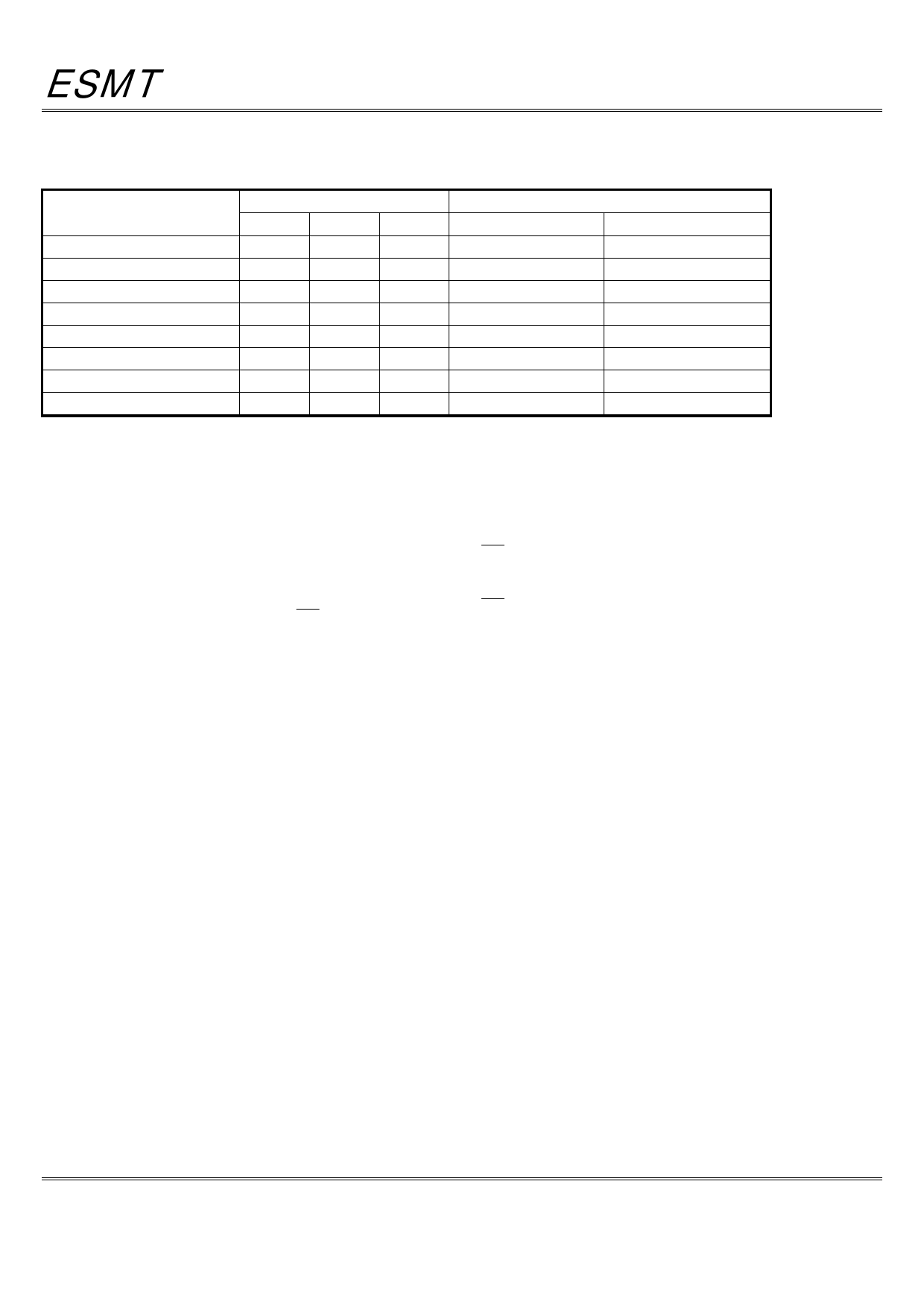
Table2 : F25L016A Block Protection Table
Protection Level
0
Upper 1/32
Upper 1/16
Upper 1/8
Upper 1/4
Upper 1/2
All Blocks
All Blocks
Status Register Bit
BP2
BP1
BP0
0
0
0
0
0
1
0
1
0
0
1
1
1
0
0
1
0
1
1
1
0
1
1
1
Protected Memory Area
Block Range
Address Range
None
None
Block 31
1F0000H – 1FFFFFH
Block 30~31
1E0000H – 1FFFFFH
Block 28~31
1C0000H – 1FFFFFH
Block 24~31
180000H – 1FFFFFH
Block 16~31
100000H – 1FFFFFH
Block 0~31
000000H – 1FFFFFH
Block 0~31
000000H – 1FFFFFH
Block Protection (BP2, BP1, BP0)
The Block-Protection (BP2, BP1, BP0) bits define the size of the
memory area, as defined in Table2 to be software protected
against any memory Write (Program or Erase) operations. The
Write-Status-Register (WRSR) instruction is used to program the
BP2, P1, BP0 bits as long as WP is high or the
Block-Protection-Look (BPL) bit is 0. Chip-Erase can only be
executed if Block-Protection bits are all 0. After power-up, BP2,
BP1 and BP0 are set to1.
Block Protection Lock-Down (BPL)
WP pin driven low (VIL), enables the Block-Protection
-Lock-Down (BPL) bit. When BPL is set to 1, it prevents any
further alteration of the BPL, BP2, BP1, and BP0 bits. When the
WP pin is driven high (VIH), the BPL bit has no effect and its
value is “Don’t Care”. After power-up, the BPL bit is reset to 0.
Elite Semiconductor Memory Technology Inc.
Publication Date: Jul. 2008
Revision: 1.4
6/32
Share Link: 