HD74ACT107 データシートの表示(PDF) - Renesas Electronics
部品番号
コンポーネント説明
メーカー
HD74ACT107 Datasheet PDF : 7 Pages
| |||
HD74AC107/HD74ACT107
Dual JK Flip-Flop (with Separate Clear and Clock)
REJ03D0243–0200Z
(Previous ADE-205-363 (Z))
Rev.2.00
Jul.16.2004
Description
The HD74AC107/HD74ACT107 dual JK master/slave flip-flops have a separate clock for each flip-flop. Inputs to the
master section are controlled by the clock pulse. The clock pulse also regulates the state of the coupling transistors
which connect the master and slave sections. The sequence of operation is as follows: 1) isolate slave from master; 2)
enter information from J and K inputs to master; 3) disable J and K inputs; 4) transfer information from master to slave.
Features
• Outputs Source/Sink 24 mA
• HD74ACT107 has TTL-Compatible Inputs
• Ordering Information: Ex. HD74AC107
Part Name
Package Type Package Code Package Abbreviation Taping Abbreviation (Quantity)
HD74AC107FPEL SOP-14 pin (JEITA) FP-14DAV
FP
EL (2,000 pcs/reel)
HD74AC107RPEL SOP-14 pin (JEDEC) FP-14DNV
RP
EL (2,500 pcs/reel)
Notes: 1. Please consult the sales office for the above package availability.
2. The packages with lead-free pins are distinguished from the conventional products by adding V at the end of
the package code.
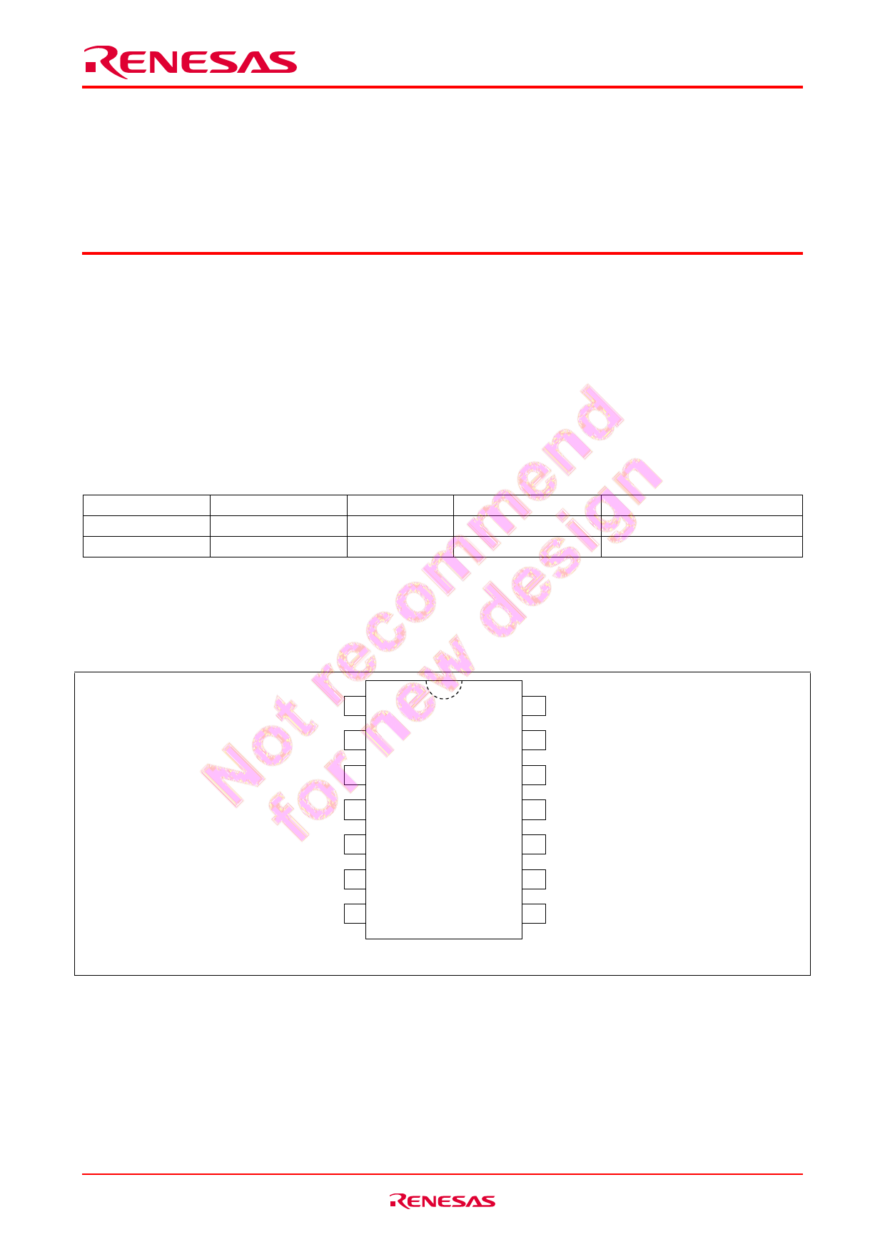
Pin Arrangement
J1 1
Q1 2
Q1 3
K1 4
Q2 5
Q2 6
GND 7
(Top view)
14 VCC
13 CD1
12 CP1
11 K2
10 CD2
9 CP2
8 J2
Rev.2.00, Jul.16.2004, page 1 of 6
Share Link: 