HD74LVC2G53CLE データシートの表示(PDF) - Renesas Electronics
部品番号
コンポーネント説明
メーカー
HD74LVC2G53CLE Datasheet PDF : 12 Pages
| |||
HD74LVC2G53
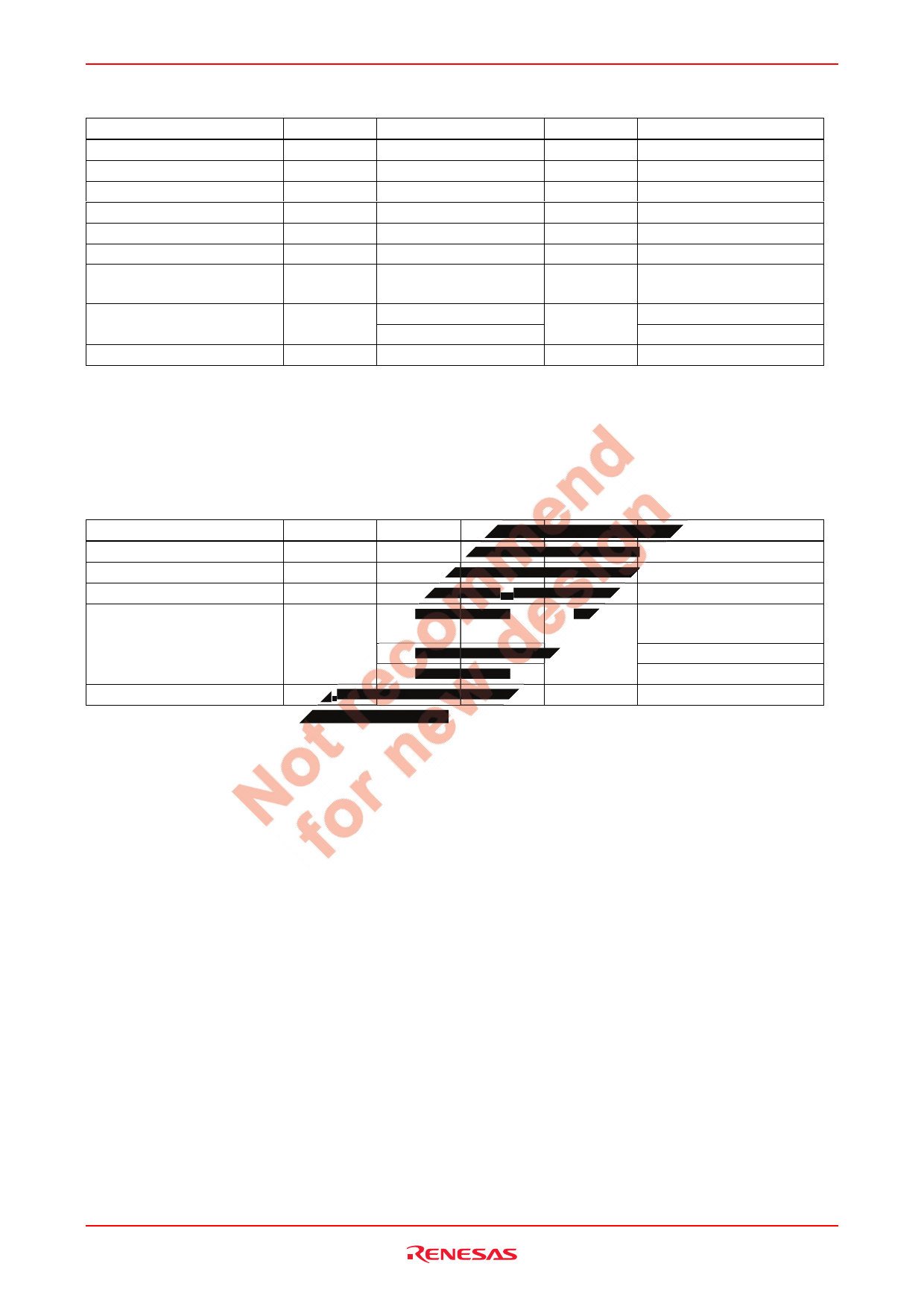
Absolute Maximum Ratings
Item
Symbol
Ratings
Unit
Test Conditions
Supply voltage range
Input voltage range *1
Output voltage range *1, 2
Input clamp current
Output clamp current
Continuous output current
Continuous current through
VCC or GND
Package Thermal impedance
VCC
VI
VO
IIK
IOK
IO
ICC or IGND
θja
–0.5 to 6.5
–0.5 to 6.5
–0.5 to VCC +0.5
–50
–50
±50
±100
140
102
V
V
V
mA
mA
mA
mA
°C/W
Output : H or L
VI < 0
VO < 0
VO = 0 to VCC
CP
CL
Storage temperature
Tstg
–65 to 150
°C
Notes:
The absolute maximum ratings are values, which must not individually be exceeded, and furthermore no two
of which may be realized at the same time.
1. The input and output voltage ratings may be exceeded if the input and output clamp-current ratings are
observed.
2. This value is limited to 5.5 V maximum.
Recommended Operating Conditions
Item
Symbol
Min
Max
Supply voltage range
VCC
1.65
5.5
Input voltage range
VI
0
5.5
Output voltage range
VO
0
VCC
Input transition rise or fall rate
∆t / ∆v
0
20
0
10
0
10
Operating free-air temperature
Ta
–40
85
Note: Unused or floating inputs must be held high or low.
Unit
V
V
V
ns / V
°C
Conditions
VCC = 1.65 to 1.95 V,
2.3 to 2.7 V
VCC = 3.0 to 3.6 V
VCC = 4.5 to 5.5 V
Rev.3.00 Jul 07, 2005 page 3 of 11
Share Link: 