LT1962EMS8 データシートの表示(PDF) - Linear Technology
部品番号
コンポーネント説明
メーカー
LT1962EMS8 Datasheet PDF : 16 Pages
| |||
LT1962 Series
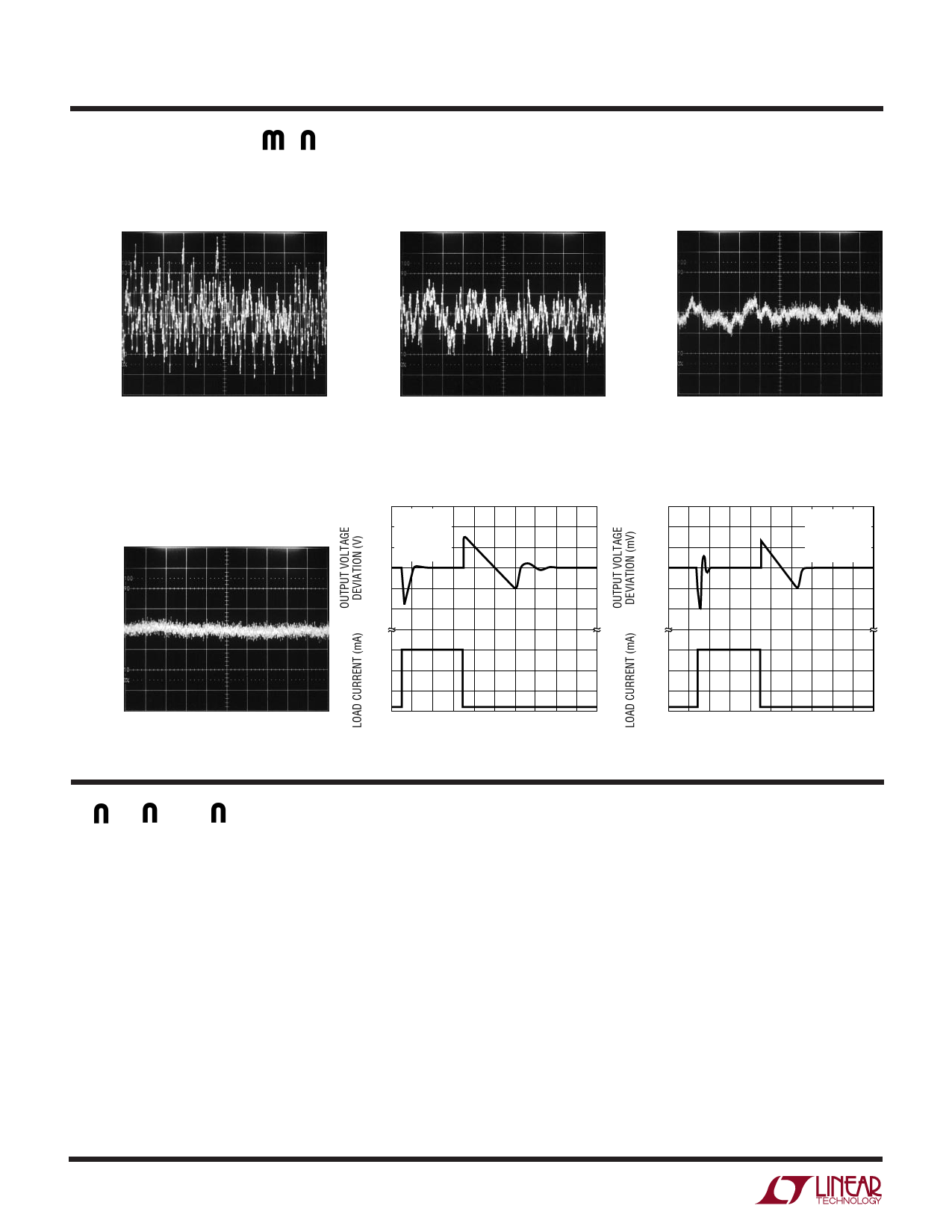
TYPICAL PERFOR A CE CHARACTERISTICS
LT1962-5 10Hz to 100kHz
Output Noise (CBYP = 0)
LT1962-5 10Hz to 100kHz
Output Noise (CBYP = 100pF)
LT1962-5 10Hz to 100kHz
Output Noise (CBYP = 1000pF)
VOUT
100µV/DIV
VOUT
100µV/DIV
VOUT
100µV/DIV
COUT = 10µF
IL = 300mA
1ms/DIV
1962 G52
COUT = 10µF
IL = 300mA
1ms/DIV
1962 G53
COUT = 10µF
IL = 300mA
1ms/DIV
1962 G54
LT1962-5 10Hz to 100kHz
Output Noise (CBYP = 0.01µF)
VOUT
100µV/DIV
COUT = 10µF
IL = 300mA
1ms/DIV
1962 G55
LT1962-5 Transient Response
VIN = 6V
0.4 CIN = 10µF
0.2
COUT = 10µF
CBYP = 0
0
–0.2
–0.4
LT1962-5 Transient Response
0.10
0.05
0
–0.05
–0.10
VIN = 6V
CIN = 10µF
COUT = 10µF
CBYP = 0.01µF
300
200
100
0
0 0.2 0.4 0.6 0.8 1.0 1.2 1.4 1.6 1.8 2.0
TIME (ms)
1962 G56
300
200
100
0
0 50 100 150 200 250 300 350 400 450 500
TIME (µs)
1962 G57
PI FU CTIO S
OUT (Pin 1): Output. The output supplies power to the
load. A minimum output capacitor of 3.3µF is required to
prevent oscillations. Larger output capacitors will be
required for applications with large transient loads to limit
peak voltage transients. See the Applications Information
section for more information on output capacitance and
reverse output characteristics.
SENSE (Pin 2): Sense. For fixed voltage versions of the
LT1962 (LT1962-1.5/LT1962-1.8/LT1962-2.5/LT1962-3/
LT1962-3.3/LT1962-5), the SENSE pin is the input to the
error amplifier. Optimum regulation will be obtained at the
point where the SENSE pin is connected to the OUT pin of
the regulator. In critical applications, small voltage drops
are caused by the resistance (RP) of PC traces between the
regulator and the load. These may be eliminated by con-
necting the SENSE pin to the output at the load as shown
in Figure 1 (Kelvin Sense Connection). Note that the
voltage drop across the external PC traces will add to the
dropout voltage of the regulator. The SENSE pin bias
current is 10µA at the nominal rated output voltage. The
SENSE pin can be pulled below ground (as in a dual supply
system where the regulator load is returned to a negative
supply) and still allow the device to start and operate.
ADJ (Pin 2): Adjust. For the adjustable LT1962, this is the
input to the error amplifier. This pin is internally clamped
to ±7V. It has a bias current of 30nA which flows into the
10
Share Link: 