LTC2908 データシートの表示(PDF) - Linear Technology
部品番号
コンポーネント説明
メーカー
LTC2908 Datasheet PDF : 18 Pages
| |||
LTC2908
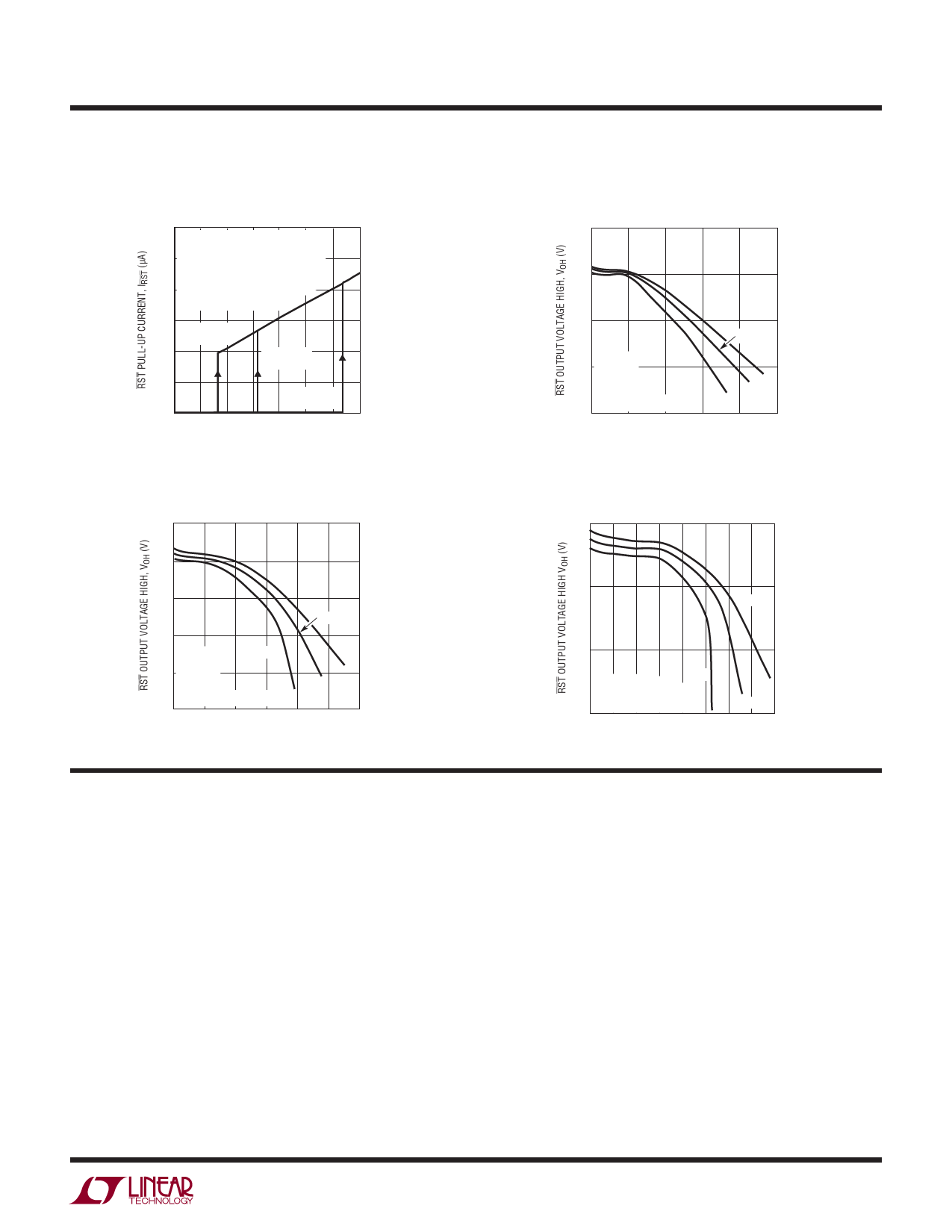
TYPICAL PERFORMANCE CHARACTERISTICS
Specifications are at TA = 25°C unless otherwise noted.
RST Pull-Up Current vs
Supply Voltage
–30
VCC = V1 = V2 (A1/B1), VCC = V1(C1)
V3 = 2.5V (A1)/V3 = 1.8V (B1)
–25 V4 = 1.8V (A1)/V4 = 1.5V (B1)
VADJ1 = VADJ2 = 0.55V (A1/B1)
–20
VADJ1 = VADJ2 = VADJ3 = VADJ4 =
RVASDTJH5 E=L0D.5A5TV(0CV1)
–15
VRT25
LTC2908-C1
–10
VRT33
LTC2908-B1
–5
VRT50
LTC2908-A1
0
1.5 2 2.5 3 3.5 4 4.5 5
SUPPLY VOLTAGE, VCC (V)
2908 G20
RST Output Voltage High vs
RST Output Source Current
LTC2908-B1
3.0
RST Output Voltage High vs
RST Output Source Current
LTC2908-A1
5
4
3
25°C
V1 = 5.0V
2 V2 = 3.3V
–40°C
V3 = 2.5V
V4 = 1.8V
VADJ1 = VADJ2 = 0.55V
1
0
–4
–8 –12
85°C
–16 –20
OUTPUT SOURCE CURRENT, IRST (μA)
2908 G21
RST Output Voltage High vs
RST Output Source Current
LTC2908-C1
2.0
2.5
2.0
25°C
1.5
V1 = 3.3V
–40°C
V2 = 2.5V
1.0 V3 = 1.8V
V4 = 1.5V
VADJ1 = VADJ2 = 0.55V
0.5
0 –2 –4 –6 –8
85°C
–10 –12
OUTPUT SOURCE CURRENT, IRST (μA)
2908 G22
1.5
85°C
1.0
V1 = 2.5V
–40°C
VADJ1 = VADJ2 = VADJ3 =
VADJ4 = VADJ5 = 0.55V
25°C
0.5
0 –1 –2 –3 –4 –5 –6 –7 –8
OUTPUT SOURCE CURRENT, IRST (μA)
2908 G24
PIN FUNCTIONS (TS8 Package/DDB8 Package) LTC2908-A1/LTC2908-B1
V2 (Pin 1/Pin 4): Voltage Input 2. The greater of V1, V2 is
also the internal VCC. The operating voltage on this pin shall
not exceed 6V. When in normal operation (V1 > V2), this pin
draws approximately 8μA. When this pin is acting as the
VCC (V2 > V1), this pin draws an additional 16μA. Bypass
this pin to ground with a 0.1μF (or greater) capacitor.
V4 (Pin 2/Pin 3): Voltage Input 4.
RST (Pin 3/Pin 2): Reset Logic Output. Pulls low when
any voltage input is below the reset threshold and is held
low for 200ms after all voltage inputs are above threshold.
This pin has a weak pull-up to VCC and may be pulled above
VCC using an external pull-up.
GND (Pin 4/Pin 1): Device Ground.
VADJ2 (Pin 5/Pin 8): Adjustable Voltage Input 2. See Table 1
for recommended ADJ resistors values.
V3 (Pin 6/Pin 7): Voltage Input 3.
VADJ1 (Pin 7/Pin 6): Adjustable Voltage Input 1. See Table 1
for recommended ADJ resistors values.
V1 (Pin 8/Pin 5): Voltage Input 1. The greater of V1, V2 is
also the internal VCC. The operating voltage on this pin shall
not exceed 6V. When in normal operation (V1 > V2), this pin
draws approximately 26 μA. When this pin is not acting as
the VCC (V2 > V1), this pin draws approximately 8μA. Bypass
this pin to ground with a 0.1μF (or greater) capacitor.
Exposed Pad (Pin 9, DDB8 Only): Exposed pad may be
left open or connected to device ground.
2908fd
7
Share Link: 