M62495AFP データシートの表示(PDF) - Renesas Electronics
部品番号
コンポーネント説明
メーカー
M62495AFP Datasheet PDF : 12 Pages
| |||
M62495AFP
Control Signals Specification
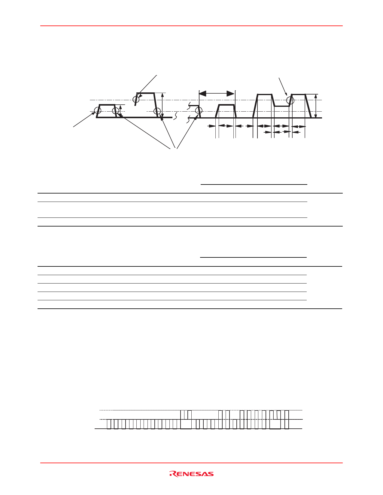
(1) Wave form
Dn+0
(CLOCK, H
DATA, M
STROBE) L
0V
DATA:L
Threshold of
the internal CLOCK.
Threshold of the internal
DATA(H/L)
Dn+1
Dn+8
Dn+9
t
or
Threshold of the internal
STROBE.
1.25V
2.5V
DATA:H
t WH
tr
tf tr
t WH
t WL
t
WH
tf
tr
2.5V
The internal DATA latch at the falling edges of this clock signal.
(2) Voltage control signal
Digital input signal
L signal
L
M signal
M
H signal
H
Condition
VDD = 2.5 V, VSS = –2.5 V
VDD = 2.5 V, VSS = –2.5 V
VDD = 2.5 V, VSS = –2.5 V
Limits
min.
typ.
max.
Unit
GND
—
0.4
V
1.0
1.25
1.5
(VDD/2)
2.1
—
VDD
(3) Timing control signal
Symbol
tcr
tWH
tWLC
tr
tf
Parameter
Cycle time of digital signal
Pulse width of digital signal (“H”level)
Pulse width of digital signal (“L”level)
Rise time of digital signal
Fall time of digital signal
Limits
min
typ
8
3.6
3.6
max
0.4
0.4
Unit
µsec
(4) Control signal example (Refer to page 6 on the control data)
An example of the mode control
INPUT
:INA
STEREO,VOLUME :0dB
BASS
:18dB
TREBLE
:6dB
RECONT
:ON
MUTE
:OFF
2.5V
(MSB)
0V
D01 D11D21D31 D41D51D61D71D81D91STROBED02 D12 D22D32 D42D52D62D72D82D92STROBED'01
(LSB)
Rev.1.00, Jul.24.2003, page 5 of 11
Share Link: 