MC78BC00(2006) データシートの表示(PDF) - ON Semiconductor
部品番号
コンポーネント説明
メーカー
MC78BC00 Datasheet PDF : 6 Pages
| |||
MC78BC00 Series
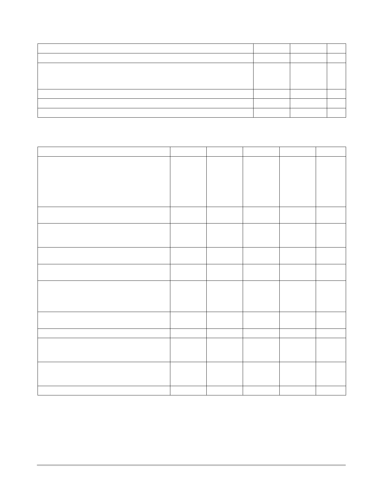
MAXIMUM RATINGS (TC = 25°C, unless otherwise noted.)
Rating
Symbol
Value
Unit
Input Voltage
VCC
10
Vdc
Power Dissipation and Thermal Characteristics Maximum Power Dissipation
Case 1212 (SOT−23) H Suffix
Thermal Resistance, Junction−to−Ambient
PD
RqJA
mW
150
333
°C/W
Operating Junction Temperature
TJ
125
°C
Operating Ambient Temperature
TA
−30 to +80
°C
Storage Temperature Range
Tstg
−40 to +125
°C
Stresses exceeding Maximum Ratings may damage the device. Maximum Ratings are stress ratings only. Functional operation above the
Recommended Operating Conditions is not implied. Extended exposure to stresses above the Recommended Operating Conditions may affect
device reliability.
NOTE: ESD data available upon request.
ELECTRICAL CHARACTERISTICS (Vin = VO + 1.0 V, IO = 50 mA, TJ = 25°C 9 (Note 2), unless otherwise noted.)
Characteristic
Symbol
Min Typ Max Unit
Output Voltage
VO
MC78BC30NTR
MC78BC31NTR
MC78BC33NTR
MC78BC40NTR
MC78BC43NTR
MC78BC45NTR
MC78BC50NTR
V
2.925 3.0 3.075
3.023 3.1 3.178
3.218 3.3 3.382
3.900 4.0 4.100
4.193 4.3 4.408
4.386 4.5 4.613
4.875 5.0 5.125
Line Regulation
VO + 0.5 V ≤ Vin ≤ 8.0 V
Load Regulation
Vin − VO = 1.0 V
1.0 mA ≤ lO ≤ 100 mA
Output Current (Note 3) Vin − VO = 1.0 V
Dropout Voltage
IO = 100 mA
Supply Current
Vin = 8.0 V
Vin − VO = 1.0 V
IO = 0 (at no load)
Supply Current (Standby) Vin = 8.0 V
Ext Leakage Current
Chip Enable Input Logic Voltage
Logic “0” (Regulator “On”)
Logic “1” (Regulator “Off”)
Regline
Regload
lO
Vin − VO
lss
0
0.1
0.3
mV
−
40
60
mV
−
1000
−
mA
−
100 200
mV
−
50
80
mA
lstandby
lLK
VCE
0.1
0.2
1.0
mA
−
−
0.5
mA
V
0
−
0.25
1.5
−
8.0
Chip Enable Input Current
VCE = 0.25 V
VCE = 1.5 V
lCEL
mA
−5.0 −3.0 −0.1
−
−
0.1
Output Voltage Temperature Coefficient
TC
−
±100
− ppm/°C
2. Low duty pulse techniques are used during test to maintain junction temperature as close to ambient as possible.
3. The output current depends upon the performance of External PNP Transistor. Use External PNP Transistor of a low saturation type, with
an HFE of 100 or more.
DEFINITIONS
Dropout Voltage − The input/output voltage differential at
which the regulator output no longer maintains regulation
against further reductions in input voltage. Measured when
the output drops 100 mV below its nominal value (which is
measured at 1.0 V differential), dropout voltage is affected by
junction temperature, load current and minimum input supply
requirements.
Line Regulation − The change in output voltage for a change
in input voltage. The measurement is made under conditions
of low dissipation or by using pulse techniques such that
average chip temperature is not significantly affected.
Load Regulation − The change in output voltage for a change
in load current at constant chip temperature.
Maximum Power Dissipation − The maximum total device
dissipation for which the regulator will operate within
specifications.
Supply Current − Current which is used to operate the
regulator chip and is not delivered to the load.
http://onsemi.com
2
Share Link: 