MF0032M-11ATXX データシートの表示(PDF) - Mitsumi
部品番号
コンポーネント説明
メーカー
MF0032M-11ATXX Datasheet PDF : 32 Pages
| |||
MITSUBISHI STORAGE CARD
Preliminary
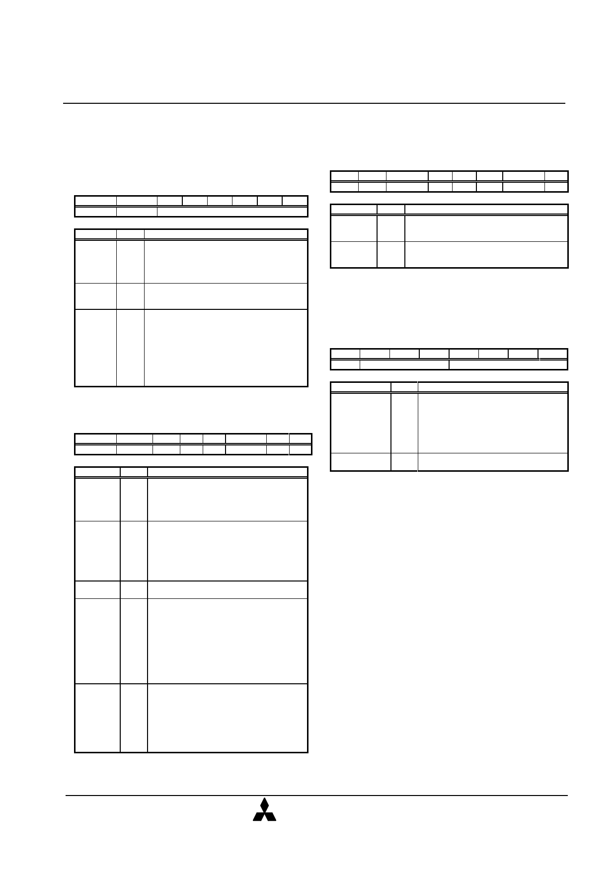
Configuration Register Specifications
Configuration Option Register
This register is used for the configuration of the card
configuration status and for the issuing soft reset to the
card.
D7
D6
D5 D4 D3 D2 D1 D0
SRESET LevIREQ
Index
Name
SRESET
LevIREQ
Index
R/W
R/W
R/W
R/W
Description
Setting this bit to “1”, places the card in the
reset state. When the host returns this bit to
“0”, the function shall enter the same
unconfigured, reset state as the card does
following a power-up and hardware reset.
If this bit is set to “0”, card generates pulse
mode interrupt. If this bit is set to “1”, card
generates level mode interrupts.
This bits is used for select operation mode of
the card as follows.
When Power on, Card Hard Reset and Soft
reset, this data is “000000” for the purpose of
Memory card interface recognition.
Index: 0 -> Memory mapped
1 -> Contiguous I/O mapped
2 -> Primary I/O mapped
3 -> Secondary I/O mapped
Configuration and Status Register
This register is used for observing the card state.
D7
D6
D5 D4 D3
D2
D1 D0
Changed SigChg Iois8 0 0 PwrDwn Intr 0
Name
Changed
SigChg
Iois8
PwrDwn
Intr
R/W
R/O
R/W
R/W
R/W
R/W
Description
This bit indicates that CREADY bit on the Pin
Replacement register is set to “1”. When
Changed bit is set to “1”, STSCHG# pin is
held “L” if the SigChg bit is “1” and the card is
configured for the I/O interface.
This bit is set or reset by the host for enabling
and disabling the status change
signal(STSCHG# pin). When the card is
configured I/O card interface and this bit is set
to “1”, STSCHG# pin is controlled by Changed
bit. If this bit is set to “0”, STSCHG# pin is
kept “H”.
This card is always configured for both 8-bit
and 16-bit I/O, so this bit is ignored.
When this bit is set to “1”, the card enters
Power Down mode. When this bit is reset to
“0”, the host is requesting the card to enter the
active mode. RREADY bit on Pin
Replacement Register becomes BUSY when
this bit is changed. RREADY will not become
Ready until the power state requested has
been entered. This card automatically powers
down when it is idle, and powers back up
when it receives a command.
This bit represents the internal state of the
interrupt request. This bit state is available
whether I/O card interface has been
configured or not. This signal remains true
until the condition which caused the interrupt
request has been serviced. If interrupts are
disabled by the nIEN bit in the Device Control
Register, this bit is a zero.
MF0XXXX-11ATXX series
ATA PC CARDS
Pin Replacement Register
This register is used for providing the signal state of
READY signal when the card configured I/O card
interface.
D7
D6
D5
D4 D3 D2
D1
D0
0
0 CREADY 0
1
1 RREADY 0
Name
CREADY
RREADY
R/W
R/W
R/W
Description
This bit is set to “1” when the RREADY bit
changes state. This bit may also be written by
the host.
When read, this bit indicates READY pin
states. When written, this bit acts as a mask
for writing the CREADY bit.
Socket and Copy Register
This register is used for identification of the card from
the other cards. Host can read and write this register.
This register should be set by host before this card’s
Configuration Option register set.
D7
D6
D5
D4
D3
D2
D1
D0
0
Copy Number
Socket Number
Name
Copy Number
Socket
Number
R/W
R/W
R/W
Description
This bit indicates the drive number of the
card for twin card configuration.
And the host can select and drive one card
by comparing the number in this field with
the drive number of Drive Head Register.
In the way, the host can perform the card’s
master/slave organization.
This field indicates to the card that it is
located in the n’th socket.
MITSUBISHI
ELECTRIC
11
June.2001 Rev. 1.3
Share Link: 