NCP1377BD1R2G データシートの表示(PDF) - ON Semiconductor
部品番号
コンポーネント説明
メーカー
NCP1377BD1R2G Datasheet PDF : 16 Pages
| |||
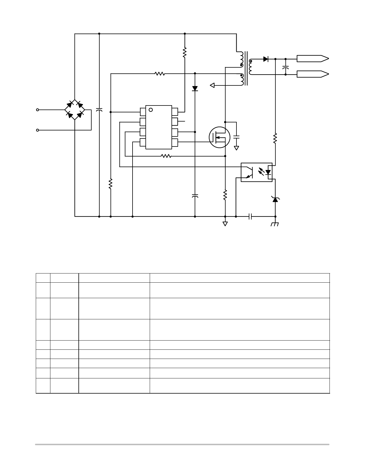
Universal
Network
NCP1377, NCP1377B
R*
OVP and NCP1377
+
Demag
1
8
2
7
3
6
4
5
12 V @ 1 A
+
GND
+
*Please refer to the application information section.
Y1 Type
Figure 1. Typical Application Schematic
PIN FUNCTION DESCRIPTION
Pin Symbol
Function
1
Demag Core reset detection and OVP
2
FB
Sets the peak current setpoint
3
CS
Current sense input and skip
cycle level selection
4
GND
5
Drv
6
VCC
7
NC
8
HV
The IC ground
Driving pulses
Supplies the IC
−
High−voltage pin
Description
The auxiliary FLYBACK signal ensures discontinuous operation and offers a fixed
overvoltage detection level of 7.2 V.
By connecting an optocoupler to this pin, the peak current setpoint is adjusted
accordingly to the output power demand. By bringing this pin below the internal
skip level, you shut off the device.
This pin senses the primary current and routes it to the internal comparator via an
L.E.B. By inserting a resistor in series with the pin, you control the level at which
the skip operation takes place.
−
The driver’s output to an external MOSFET.
This pin is connected to an external bulk capacitor of typically 10 mF.
This unconnected pin ensures adequate creepage distance.
Connected to the high−voltage rail, this pin injects a constant current into the VCC
bulk capacitor and ensures a clean lossless startup sequence.
http://onsemi.com
2
Share Link: 