SC613EVB データシートの表示(PDF) - Semtech Corporation
部品番号
コンポーネント説明
メーカー
SC613EVB Datasheet PDF : 14 Pages
| |||
POWER MANAGEMENT
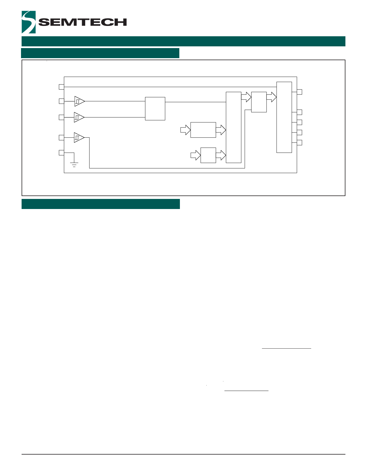
Block Diagram
VIN 3
EN 6
FSEL 45
VSEL 54
GND 8
SC613
EN
OSC
650kHz or 262kHz
VIN
VOUT
VREF
COMPARATORS
TIMER
VIN
5.0V or 4.5V
MODE
SELECT
DRIVERS
SWITCH
BLOCK
1 VOUT
2 CF1+
9 CF1-
10 CF2+
7 CF2-
Applications Information
Charge Pump Doubler Type
The SC613 uses a voltage doubler circuit which is implemented
with two switched or ‘bucket’ capactors. Most charge pump dou-
blers use only one bucket capacitor. Two bucket capacitors switch-
ing on alternate phases greatly reduce the output ripple voltage
and also reduce the size requirement for the output capacitor.
Over Voltage Protection
The output is prevented from exceeding 6.0V. This feature allows
the use of 6.3V ceramic capacitors.
Comparison with Other Regulation Methods
In many instances, a charge pump regulator is the best choice for
portable power applications. These regulators offer many advan-
tages over switch mode regulators. A smaller bill of materials,
less layout area, lower component height, less noise, no EMF, and
less overall circuit cost are typical reasons to use this type of
regulation. The efficiency of a charge pump regulator often ap-
proaches and in some cases exceeds the efficiency of a switch
mode regulator.
difficult to ensure acceptable noise performance over the entire
operating range.
Many switch mode regulators have increased voltage ripple on
the output during pulse skipping mode due to the fact that there
are large periods of time when no current is supplied to the output.
The SC613 supplies current to the output continuously, so the
voltage ripple is less than a switch mode regulator, even with greatly
reduced output capacitance.
Frequency Selection
The FSEL input is for frequency selection. A logic High level at this
input will set the clock frequency to 650kHz, while a logic Low sets
the clock to 262kHz. Input from a uP or other device may be used
to change the charge pump frequency at any time. The optimal
frequency will depend upon the capacitor values, the load current,
and the exceptable amount of output ripple.
Ripple Performance
Examples of the output ripple per charge pump frequency and
output voltage are listed in the Ripple Performance table on page
5.
Inductors are often the largest and most expensive discrete com-
ponent in a design. There are no inductors used in the SC613, so
the inductor’s cost and layout area are eliminated. The noise and
EMF associated with the inductor are also eliminated.
The SC613’s fixed frequency harmonics are an advantage in por-
table communications equipment, such as cellular telephones.
The SC613 has distinct frequencies of operation, so the harmon-
ics are predictable. The harmonics are not fixed in a switch mode
regulator. Switch mode regulators have harmonics which vary
due to the pulse width modulation used to regulate the output.
Varying harmonics can be a problem because it may be more
Efficiency
Efficiency for the SC613 is defined as,
η=
V O⋅I O
V IN⋅(2⋅I O + I Q)
where
VO = output voltage
I = output current
O
VIN = input voltage
IQ = quiescent current [from Electrical Characteristics
on page 2].
2005 Semtech Corp.
5
www.semtech.com
Share Link: 