SE1030W データシートの表示(PDF) - SiGe Semiconductor, Inc.
部品番号
コンポーネント説明
メーカー
SE1030W Datasheet PDF : 9 Pages
| |||
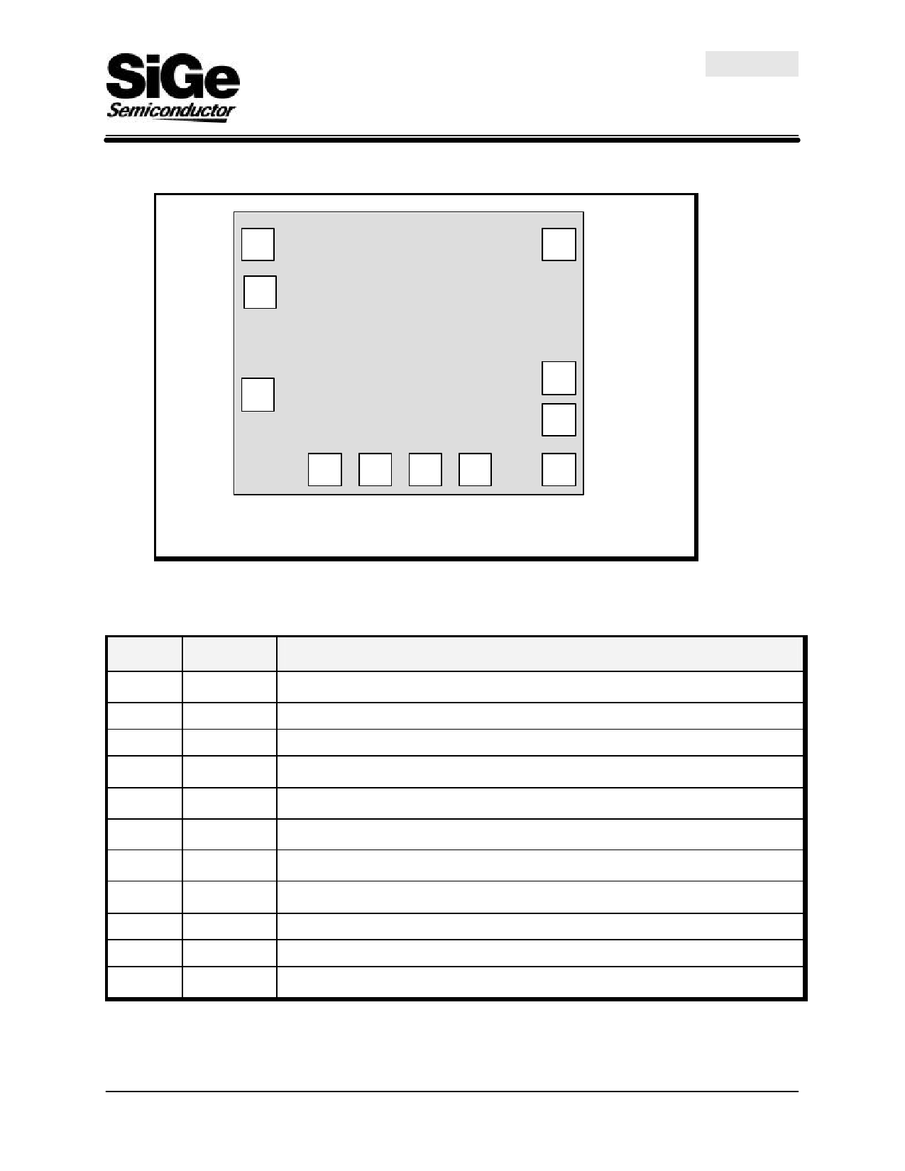
Bondpad Diagram
SE1030W
LightCharger™ 2.5 Gb/s Transimpedance Amplifier
Final
VCC
1
DNC
2
TZ_IN 3
Top
View
4
5
6
7
VEE2 VEE1 VEE1 VEE1
11 VCC
10 OUTP
9 OUTN
8
VCC
Bondpad Description
Pad No.
1
2
3
4
5
6
7
8
9
10
11
Name
VCC
DNC
TZ_IN
VEE2
VEE1
VEE1
VEE1
VCC
OUTN
OUTP
VCC
Description
Positive supply (+3.3 V), pads 1, 8 & 11 are connected on chip. Only one pad needs
to be bonded.
Do not connect.
Input pad (connect to photodetector anode).
Negative supply (0V) – Note this is separate ground for the input stage, which is AC
coupled on chip. There is no DC current through this pad.
Negative supply (0V), pads 5, 6 & 7 are connected on chip. Only one pad needs to be
bonded.
Negative supply (0V), pads 5, 6 & 7 are connected on chip. Only one pad needs to be
bonded.
Negative supply (0V), pads 5, 6 & 7 are connected on chip. Only one pad needs to be
bonded.
Positive supply (+3.3 V), pads 1, 8 & 11 are connected on chip. Only one pad needs
to be bonded.
Negative differential voltage output.
Positive differential voltage output.
Positive supply (+3.3 V), pads 1, 8 & 11 are connected on chip. Only one pad needs
to be bonded.
43-DST-01 § Rev 1.5 § May 24/02
2 of 9
Share Link: 