NUP2115LT1G データシートの表示(PDF) - ON Semiconductor
部品番号
コンポーネント説明
メーカー
NUP2115LT1G Datasheet PDF : 5 Pages
| |||
NUP2115L, SZNUP2115L
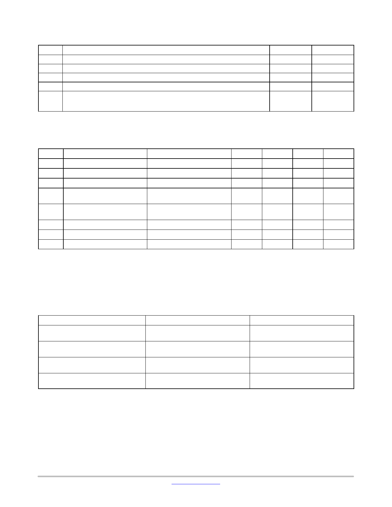
MAXIMUM RATINGS (TJ = 25°C, unless otherwise specified)
Symbol
Rating
Value
Unit
PPK Peak Power Dissipation, 8 x 20 ms Double Exponential Waveform (Note 1)
200
W
TJ
TJ
TL
ESD
Operating Junction Temperature Range
Storage Temperature Range
Lead Solder Temperature (10 s)
Human Body Model (HBM)
Machine Model (MM)
IEC 61000−4−2 Specification (Contact)
−55 to 150
°C
−55 to 150
°C
260
°C
8.0
kV
400
V
30
kV
Stresses exceeding those listed in the Maximum Ratings table may damage the device. If any of these limits are exceeded, device functionality
should not be assumed, damage may occur and reliability may be affected.
1. Non−repetitive current pulse per Figure 1.
ELECTRICAL CHARACTERISTICS (TJ = 25°C, unless otherwise specified)
Symbol
Parameter
Test Conditions
Min
Typ
Max
Unit
VRWM
VBR
IR
VC
Reverse Working Voltage
Breakdown Voltage
Reverse Leakage Current
Clamping Voltage
(Note 2)
IT = 1 mA (Note 3)
VRWM = 24 V
IPP = 1 A (8/20 ms Waveform)
(Note 4)
24
−
−
V
26.2
−
32
V
−
15
100
nA
−
33.4
36.6
V
VC Clamping Voltage
IPP = 3 A (8/20 ms Waveform)
(Note 4)
−
44
50
V
IPP Maximum Peak Pulse Current
8/20 ms Waveform (Note 4)
−
−
3.0
A
CJ
Capacitance
VR = 0 V, f = 1 MHz (Line to GND)
−
−
10
pF
DC Diode Capacitance Matching
VR = 0 V, 5 MHz (Note 5)
−
0.1
2
%
Product parametric performance is indicated in the Electrical Characteristics for the listed test conditions, unless otherwise noted. Product
performance may not be indicated by the Electrical Characteristics if operated under different conditions.
2. Surge protection devices are normally selected according to the working peak reverse voltage (VRWM), which should be equal or greater
than the DC or continuous peak operating voltage level.
3. VBR is measured at pulse test current IT.
4. Pulse waveform per Figure 1.
5. DC is the percentage difference between CJ of lines 1 and 2 measured according to the test conditions given in the electrical characteristics
table.
ORDERING INFORMATION
Device
Package
Shipping†
NUP2115LT1G
SOT−23
(Pb−Free)
3,000 / Tape & Reel
SZNUP2115LT1G
SOT−23
(Pb−Free)
3,000 / Tape & Reel
NUP2115LT3G
SOT−23
(Pb−Free)
10,000 / Tape & Reel
SZNUP2115LT3G
SOT−23
(Pb−Free)
10,000 / Tape & Reel
†For information on tape and reel specifications, including part orientation and tape sizes, please refer to our Tape and Reel Packaging
Specifications Brochure, BRD8011/D.
www.onsemi.com
2
Share Link: 