VN920-E データシートの表示(PDF) - STMicroelectronics
部品番号
コンポーネント説明
メーカー
VN920-E Datasheet PDF : 24 Pages
| |||
VN920-E / VN920B5-E / VN920SO-E
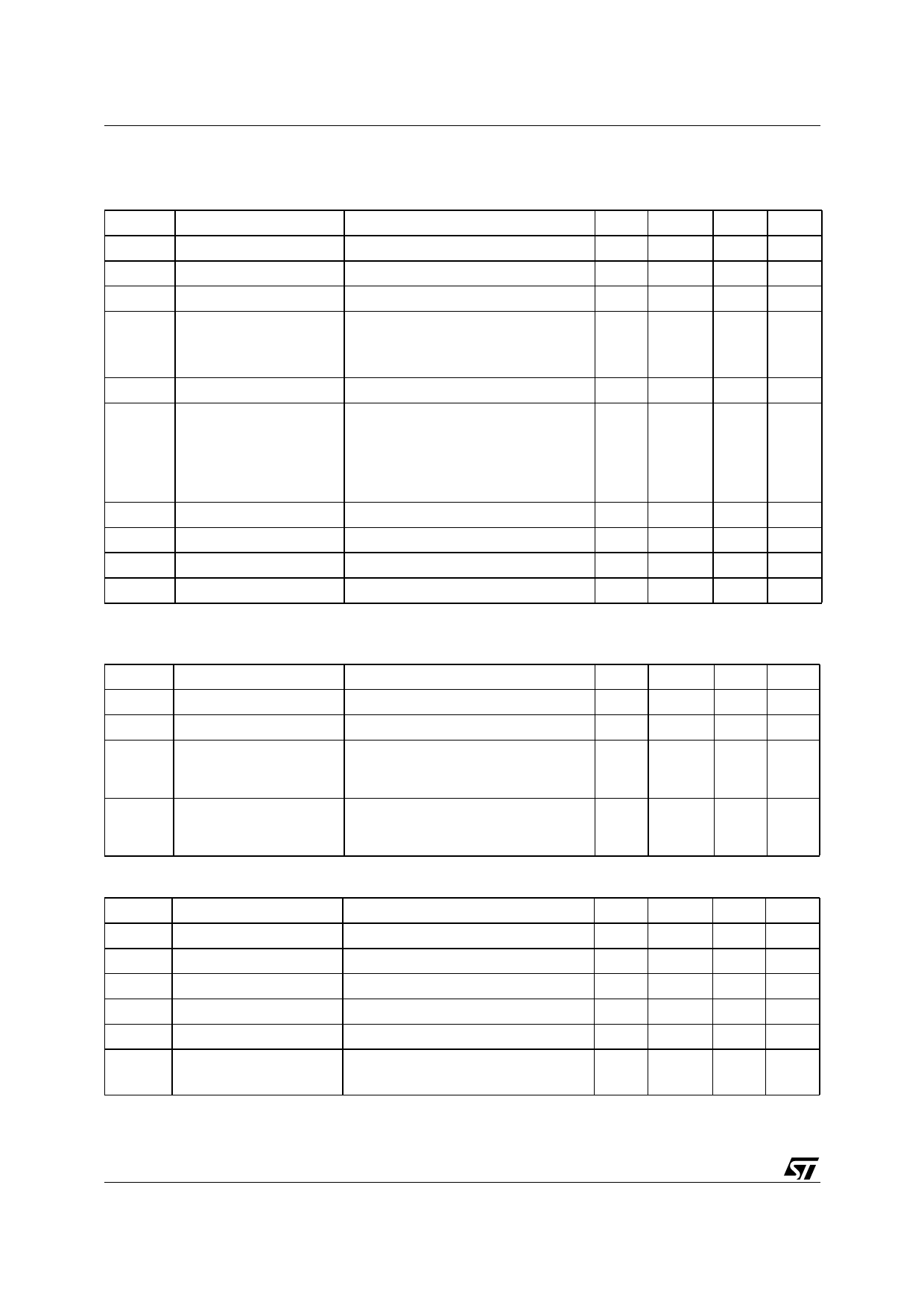
ELECTRICAL CHARACTERISTICS (8V<VCC<36V; -40°C<Tj<150°C unless otherwise specified)
Table 5. Power
Symbol
Parameter
Test Conditions
VCC
VUSD
Operating Supply Voltage
Undervoltage Shut-down
VOV
RON
Overvoltage Shut-down
On State Resistance
IOUT=10A; Tj=25°C
IOUT=10A
IOUT=3A; VCC=6V
Vclamp Clamp Voltage
ICC=20mA (See note 1)
Supply Current
IS
Off State; VCC=13V; VIN=VOUT=0V
Off State; VCC=13V; VIN=VOUT=0V;
Tj=25°C
On State; VCC=13V; VIN=5V; IOUT=0A;
RSENSE=3.9KΩ
IL(off1)
IL(off2)
Off State Output Current
Off State Output Current
VIN=VOUT=0V
VIN=0V; VOUT=3.5V
IL(off3) Off State Output Current VIN=VOUT=0V; VCC=13V; Tj=125°C
IL(off4) Off State Output Current VIN=VOUT=0V; VCC=13V; Tj=25°C
Note: 1. Vclamp and VOV are correlated. Typical difference is 5V.
Min.
5.5
3
36
41
0
-75
Typ.
13
4
48
10
10
Max.
36
5.5
16
32
55
55
25
20
Unit
V
V
V
mΩ
mΩ
mΩ
V
µA
µA
5
mA
50
µA
0
µA
5
µA
3
µA
Table 6. Switching (VCC =13V)
Symbol
Parameter
td(on) Turn-on Delay Time
td(off) Turn-off Delay Time
dVOUT/
dt(on)
Turn-on Voltage Slope
Test Conditions
RL=1.3Ω (see figure 6)
RL=1.3Ω (see figure 6)
RL=1.3Ω (see figure 6)
dVOUT/
dt(off)
Turn-off Voltage Slope
RL=1.3Ω (see figure 6)
Min.
Typ.
50
50
See
relative
diagram
See
relative
diagram
Max.
Unit
µs
µs
V/µs
V/µs
Table 7. Logic Input
Symbol
Parameter
VIL
Input Low Level
IIL
Low Level Input Current
VIH
Input High Level
IIH
High Level Input Current
VI(hyst) Input Hysteresis Voltage
VICL Input Clamp Voltage
Test Conditions
VIN=1.25V
VIN=3.25V
IIN=1mA
IIN=-1mA
Min.
1
3.25
0.5
6
Typ.
6.8
-0.7
Max.
1.25
10
8
Unit
V
µA
V
µA
V
V
V
4/24
Share Link: 