CX28HC64DMB-12(2006) データシートの表示(PDF) - Intersil
部品番号
コンポーネント説明
メーカー
CX28HC64DMB-12 Datasheet PDF : 17 Pages
| |||
X28HC64
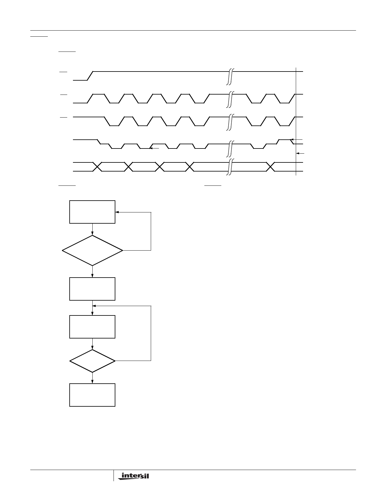
PIN DESCRIPTIONS
Addresses (A0-A12)
The Address inputs select an 8-bit memory location
during a read or write operation.
Chip Enable (CE)
The Chip Enable input must be LOW to enable all
read/write operations. When CE is HIGH, power con-
sumption is reduced.
Output Enable (OE)
The Output Enable input controls the data output buff-
ers and is used to initiate read operations.
PIN NAMES
Symbol
A0-A12
I/O0-I/O7
WE
CE
OE
VCC
VSS
NC
Data In/Data Out (I/O0-I/O7)
Data is written to or read from the X28HC64 through
the I/O pins.
Write Enable (WE)
The Write Enable input controls the writing of data to
the X28HC64.
BLOCK DIAGRAM
A0–A12
Address
Inputs
X Buffers
Latches and
Decoder
Y Buffers
Latches
and
Decoder
65,536-Bit
EEPROM
Array
I/O Buffers
and Latches
CE
Control
OE
Logic and
WE
Timing
VCC
VSS
I/O0–I/O7
Data Inputs/Outputs
Description
Address Inputs
Data Input/Output
Write Enable
Chip Enable
Output Enable
+5V
Ground
No Connect
4
FN8109.1
June 7, 2006
Share Link: 