CXA2566M データシートの表示(PDF) - Sony Semiconductor
部品番号
コンポーネント説明
メーカー
CXA2566M Datasheet PDF : 12 Pages
| |||
CXA2566M
Description of Operation
1) Det Pin (Pin 7)
This is the external pin for the detector during AVLS mode. The attack time is determined by the internal
charging buffer and the external capacitor. The recovery time is determined by both the 80k impedance inside
the IC and the external capacitor.
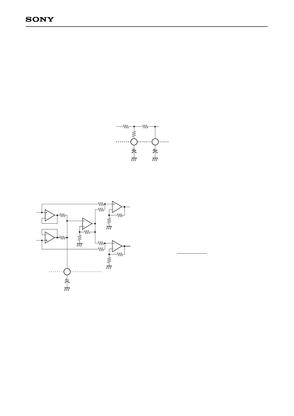
2) RF_Out (Pin 9) / RF_In (Pin 10)
These are the two external pin for the power supply's ripple filter. It provides a regulated 0.92 × Vcc to the
internal circuits. The rejection ratio is determined by the resistors inside the IC and the two external capacitors.
32k
VCC
100k
368k
VCC
Regulated
10
RF_In
9
RF_Out
3) C Pin (Pin 13)
Left
32k
32k
32k
32k
Right
32k
21k 65k 32k
13
C
32k
32k
Out
Left
32k
The bass boost circuitry is designed to provide a 9dB
gain at 100Hz for C = 0.1µF.
The cut off frequency is determined by:
Out
Right
32k
1
fcutoff =
2π × 16k × C
–9–
Share Link: 