MC74AC174D データシートの表示(PDF) - Motorola => Freescale
部品番号
コンポーネント説明
メーカー
MC74AC174D Datasheet PDF : 7 Pages
| |||
MC74AC174 MC74ACT174
FUNCTIONAL DESCRIPTION
The MC74AC174/74ACT174 consists of six edge-triggered D
flip-flops with individual D inputs and Q outputs. The Clock
(CP) and Master Reset (MR) are common to all flip-flops. Each
D input’s state is transferred to the corresponding flip-flop’s
output following the LOW-to-HIGH Clock (CP) transition. A
LOW input to the Master Reset (MR) will force all outputs LOW
independent of Clock or Data inputs. The MC74AC174/
74ACT174 is useful for applications where the true output only
is required and the Clock and Master Reset are common to all
storage elements.
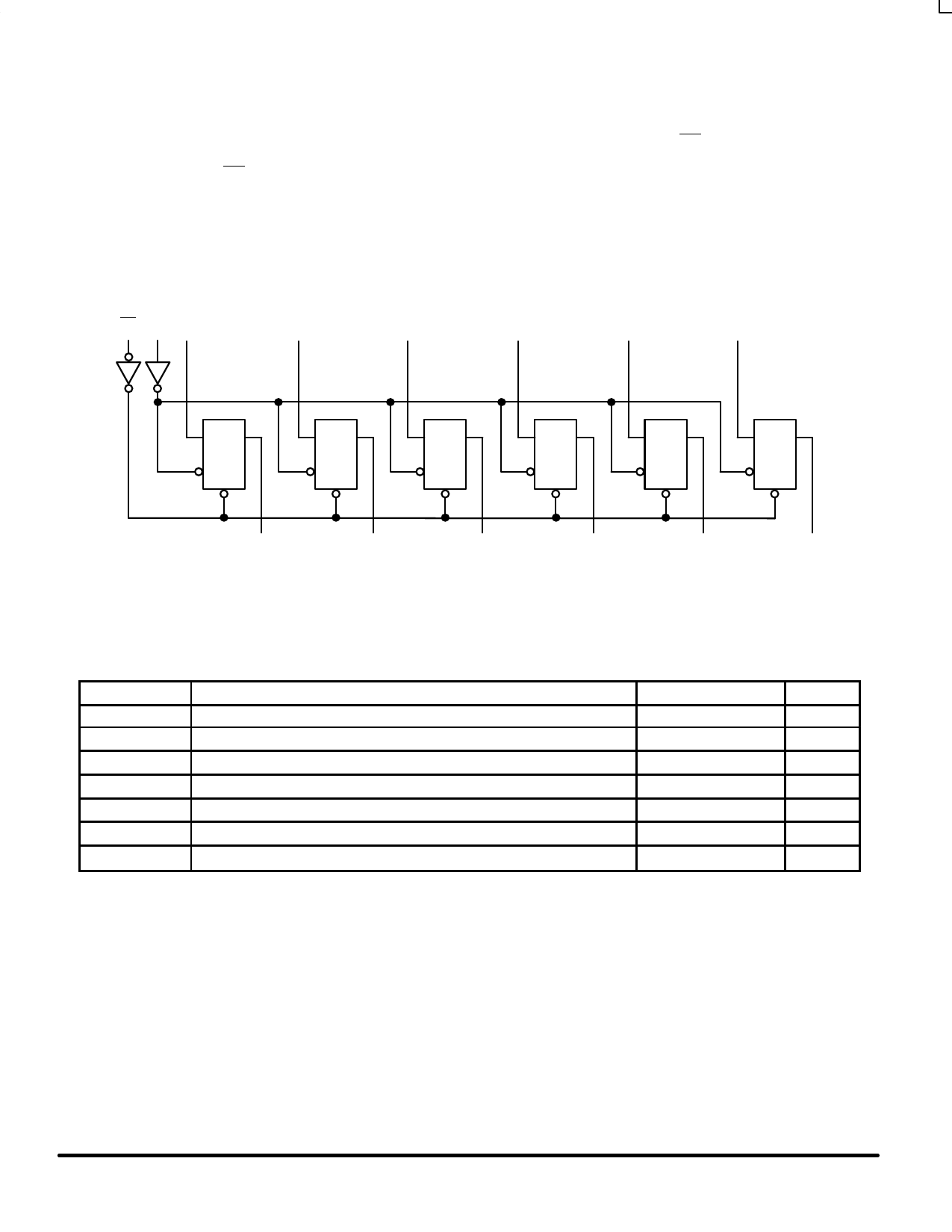
LOGIC DIAGRAM
MR CP D5
D4
D3
D2
D1
D0
DQ
CP
CD
DQ
CP
CD
DQ
CP
CD
DQ
CP
CD
DQ
CP
CD
DQ
CP
CD
Q5
Q4
Q3
Q2
Q1
Q0
Please note that this diagram is provided only for the understanding of logic
operations and should not be used to estimate propagation delays.
MAXIMUM RATINGS*
Symbol
Parameter
Value
Unit
VCC
Vin
Vout
Iin
Iout
ICC
Tstg
DC Supply Voltage (Referenced to GND)
DC Input Voltage (Referenced to GND)
DC Output Voltage (Referenced to GND)
DC Input Current, per Pin
DC Output Sink/Source Current, per Pin
DC VCC or GND Current per Output Pin
Storage Temperature
–0.5 to +7.0
V
–0.5 to VCC +0.5
V
–0.5 to VCC +0.5
V
±20
mA
±50
mA
±50
mA
–65 to +150
°C
* Maximum Ratings are those values beyond which damage to the device may occur. Functional operation should be restricted to the Recommended
Operating Conditions.
FACT DATA
5-2
Share Link: 