M50FW002 データシートの表示(PDF) - STMicroelectronics
部品番号
コンポーネント説明
メーカー
M50FW002 Datasheet PDF : 39 Pages
| |||
M50FW002
dictable results may occur. Care should be taken
to avoid unpredictable behavior by changing WP
during Program or Erase Suspend.
Reserved for Future Use (RFU). These pins do
not have assigned functions in this revision of the
part. They must be left disconnected.
Address/Address Multiplexed (A/A Mux)
Signal Descriptions
For the Address/Address Multiplexed (A/A Mux)
Interface see Figure 4, and Table 2.
Address Inputs (A0-A10). The Address Inputs
are used to set the Row Address bits (A0-A10) and
the Column Address bits (A11-A17). They are
latched during any bus operation by the Row/Col-
umn Address Select input, RC.
Data Inputs/Outputs (DQ0-DQ7). The Data In-
puts/Outputs hold the data that is written to or read
from the memory. They output the data stored at
the selected address during a Bus Read opera-
tion. During Bus Write operations they represent
the commands sent to the Command Interface of
the internal state machine. The Data Inputs/Out-
puts, DQ0-DQ7, are latched during a Bus Write
operation.
Output Enable (G). The Output Enable, G, con-
trols the Bus Read operation of the memory.
Write Enable (W). The Write Enable, W, controls
the Bus Write operation of the memory’s Com-
mand Interface.
Row/Column Address Select (RC). The Row/
Column Address Select input selects whether the
Address Inputs should be latched into the Row
Address bits (A0-A10) or the Column Address bits
(A11-A17). The Row Address bits are latched on
the falling edge of RC whereas the Column
Address bits are latched on the rising edge.
Ready/Busy Output (RB). The Ready/Busy pin
gives the status of the memory’s Program/Erase
Controller. When Ready/Busy is Low, VOL, the
memory is busy with a Program or Erase operation
and it will not accept any additional Program or
Erase command except the Program/Erase
Suspend command. When Ready/Busy is High,
VOH, the memory is ready for any Read, Program
or Erase operation.
Supply Signal Descriptions
The Supply Signals are the same for both interfac-
es.
VCC Supply Voltage. The VCC Supply Voltage
supplies the power for all operations (Read, Pro-
gram, Erase etc.).
The Command Interface is disabled when the VCC
Supply Voltage is less than the Lockout Voltage,
VLKO. This prevents Bus Write operations from
accidentally damaging the data during power up,
power down and power surges. If the Program/
Erase Controller is programming or erasing during
this time then the operation aborts and the
memory contents being altered will be invalid.
After VCC becomes valid the Command Interface
is reset to Read mode.
A 0.1µF capacitor should be connected between
the VCC Supply Voltage pins and the VSS Ground
pin to decouple the current surges from the power
supply. Both VCC Supply Voltage pins must be
connected to the power supply. The PCB track
widths must be sufficient to carry the currents
required during program and erase operations.
VPP Optional Supply Voltage. The VPP Optional
Supply Voltage pin is used to select the Fast
Program (see the Quadruple Byte Program
Command description) and Fast Erase options of
the memory and to protect the memory. When VPP
< VPPLK Program and Erase operations cannot be
performed and an error is reported in the Status
Register if an attempt to change the memory
contents is made. When VPP = VCC Program and
Erase operations take place as normal. When VPP
= VPPH Fast Program (if A/A Mux interface is
selected) and Fast Erase operations are used.
Any other voltage input to VPP will result in
undefined behavior and should not be used.
VPP should not be set to VPPH for more than 80
hours during the life of the memory.
VSS Ground. VSS is the reference for all the volt-
age measurements.
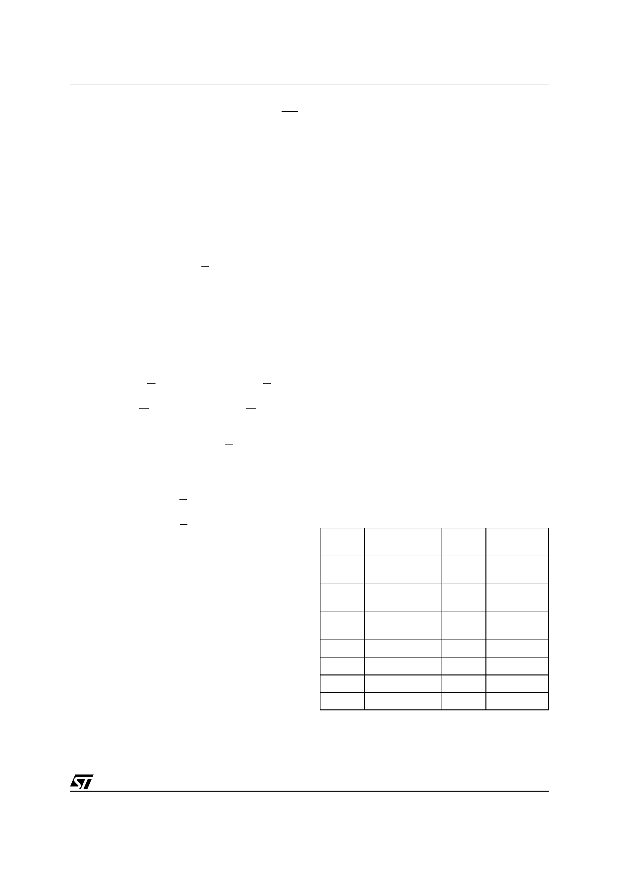
Table 3. Block Addresses
Size
(Kbytes)
Address Range
Block
Number
16 3C000h-3FFFFh
6
8
3A000h-3BFFFh
5
8
38000h-39FFFh
4
32 30000h-37FFFh
3
64 20000h-2FFFFh
2
64 10000h-1FFFFh
1
64 00000h-0FFFFh
0
Block Type
Boot Block
(Top)
Parameter
Block
Parameter
Block
Main Block
Main Block
Main Block
Main Block
7/39
Share Link: 