ST93C06 データシートの表示(PDF) - STMicroelectronics
部品番号
コンポーネント説明
メーカー
ST93C06 Datasheet PDF : 15 Pages
| |||
ST93C06, ST93C06C
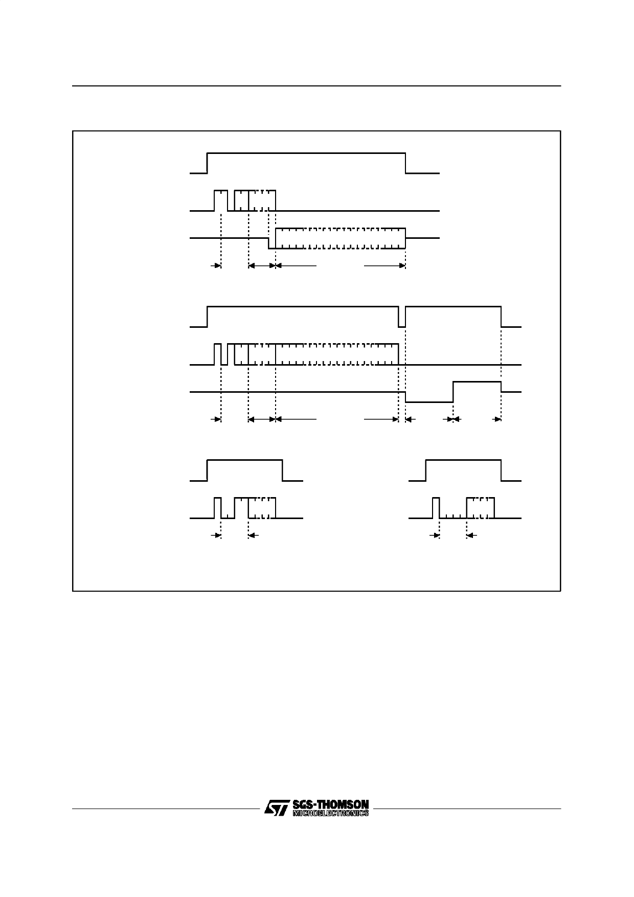
Figure 6. READ, WRITE, EWEN, EWDS Sequences
READ
S
D
1 1 0 X X An A0
Q
Qn
Q0
OP
CODE ADDR
DATA OUT
WRITE
S
D
Q
1 0 1 X X An A0 Dn
CHECK
STATUS
D0
OP
CODE ADDR
DATA IN
BUSY
READY
ERASE
S
WRITE
ENABLE
D
1 0 0 1 1 Xn X0
ERASE S
WRITE
DISABLE
D
1 0 0 0 0 Xn X0
OP
CODE
OP
CODE
AI00822D
Notes: 1. An: n = 3 for x16 org. and 4 for x8 org.
2. Xn: n = 3 for x16 org. and 4 for x8 org.
If the ST93C06 is still performing the erase cycle,
the Busy signal (Q = 0) will be returned if S is driven
high, and the ST93C06 will ignore any data on the
bus. When the erase cycle is completed, the Ready
signal (Q = 1) will indicate (if S is driven high) that
the ST93C06 is ready to receive a new instruction.
Write
The Write instruction (WRITE) is followed by the
address and the 8 or 16 data bits to be written. Data
input is sampled on the Low to High transition of
the clock. After the last data bit has been sampled,
Chip Select (S) must be brought Low before the
next rising edge of the clock (C) in order to start the
self-timed programming cycle. If the ST93C06 is
still performing the write cycle, the Busy signal (Q
= 0) will be returned if S is driven high, and the
ST93C06 will ignore any data on the bus. When the
write cycle is completed, the Ready signal (Q = 1)
will indicate (if S is driven high) that the ST93C06
is ready to receive a new instruction. Programming
is internally self-timed (the external clock signal on
C input may be disconnected or left running after
the start of a programming cycle) and does not
require an Erase instruction prior to the Write in-
struction (The Write instruction includes an auto-
matic erase cycle before programing data).
7/15
Share Link: 