ILC6360CIR-36 データシートの表示(PDF) - Impala Linear Corporation
部品番号
コンポーネント説明
メーカー
ILC6360CIR-36
Impala Linear Corporation

ILC6360CIR-36 Datasheet PDF : 14 Pages
| |||
Step-Up/Step-Down DC-DC Converter for 1-Cell Lithium-Ion Batteries
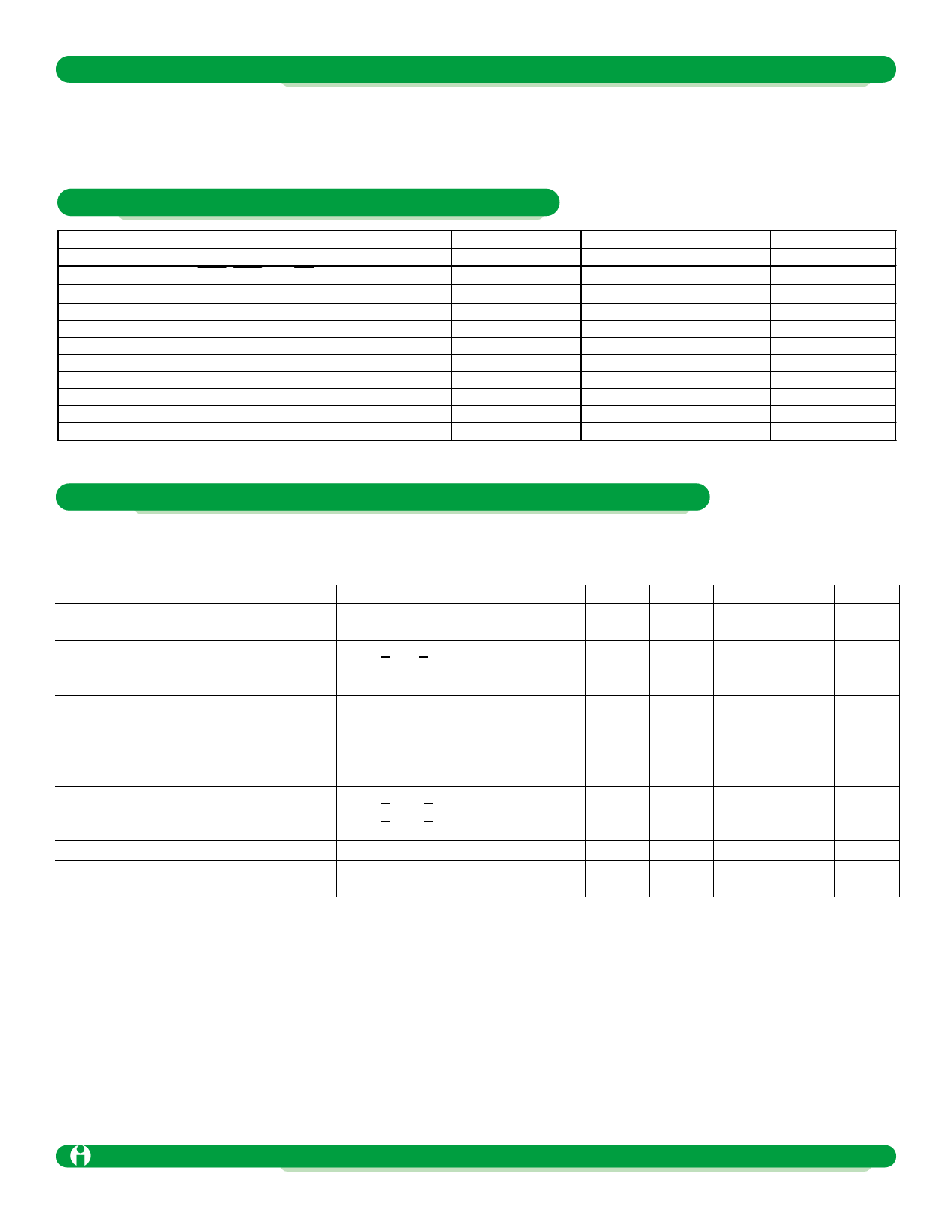
Absolute Maximum Ratings (Note 1)
Parameter
Voltage on VOUT pin
Voltage on LBI, Sync, LBO, POK, LBI/SD, VFB, LX and VIN pins
Peak switch current on LX pin
Current on LBO pin
Continuous total power dissipation at 85°C
Short circuit duration
Operating ambient temperature
Maximum junction temperature
Storage temperature
Lead temperature (soldering 10 sec)
Package thermal resistance
Symbol
VOUT
-
ILX
Isink(LBO)
Pd
ISC
TA
TJ (max)
Tstg
θJA
Ratings
-0.3 to 7
-0.3 to 7
1
5
400
1
-40 to 85
170
-40 to 125
300
206
Units
V
V
A
mA
mW
sec
°C
°C
°C
°C
°C/W
Electrical Characteristics ILC6360CIR-36 and ILC6360CIR-ADJ
Unless otherwise specified all limits are at TA = 25°C, VIN = 3.6V, VOUT = 3.6V, VLBI = 1.5V, IOUT = 1mA, FOSC = 300kHz.
Test circuit of figure 2 for ILC6360-36 and test circuit of figure 9 for ILC6360-ADJ. BOLDFACE type indicates limits that
apply over the full operating temperature range. Note 2.
Parameter
Input Voltage
Output Voltage
Feedback Voltage
(ILC6360-ADJ only)
Output Voltage
Adjustment Range
ILC6360CIR-ADJ only
Output Current
Load Regulation
Efficiency
No Load Battery Input
Current
Symbol
VIN
VOUT
VFB
Conditions
VOUT = VOUT(nominal) ± 4%
(Note 3)
2.8V < VIN < 4.2V, IOUT = 0mA
VOUT (adj) min
VOUT (adj) max
VIN = 3.3V, IOUT = 50mA
IOUT
∆VOUT
VOUT (no λοαδ)
η
IIN (no load)
VIN = 3.6V, VOUT = VOUT(nom) ± 4%
(Note 3)
0mA < IOUT < 500mA
0mA < IOUT < 300mA
0mA < IOUT < 200mA
IOUT = 300mA
IOUT = 0mA
Min
2.7
3.528
1.225
1.212
Typ
3.600
1.250
2.5
6
Max
VOUT (nom) +0.8
3.672
1.275
1.288
Units
V
V
V
V
500
mA
4
%
1
1
93
%
250
µA
Impala Linear Corporation
ILC6360 1.1
(408) 574-3939 www.impalalinear.com
Jan 1999 3
Share Link: