TDA7256 データシートの表示(PDF) - STMicroelectronics
部品番号
コンポーネント説明
メーカー
TDA7256 Datasheet PDF : 10 Pages
| |||
TDA7256
ELECTRICAL CHARACTERISTICS (VS = 14.4V, RL = 4Ω, f = 1KHz; Tamb = 25°C, unless otherwise
specified)
Symbol
Parameter
Test Condition
Min. Typ. Max. Unit
VS
Supply Voltage
8
18
V
Iq
Quiescent Drain Current
80
150 mA
Ri
Input Resistance
50
KΩ
CMR
Common Mode Rejection
f = 1KHz, Vin = 100mV
60
dB
VOS
Output Offset Voltage
150 mV
Po
Output Power
d = 10%
RL = 4Ω
RL = 3.2Ω
RL = 2Ω
18
22
W
26
W
30
W
d
Distortion
Po = 0.1W to 13W
0.05 0.5
%
GV
Voltage Gain (CL)
36
dB
eN
Total Input Noise Voltage
Rg = 10KΩ, B = 22Hz to 22KHz
3
10
µV
SVR
Supply Voltage Rejection
Rg = 10KΩ, Vr = 1Vrms,
45
60
dB
f = 300Hz
Muting Attenuation
Vref = 1Vrms,
60
dB
f = 100Hz to 10KHz
Muting-in Threshold Voltage
Pin 1
2.4
V
Muting-out Threshold Voltage
Pin 1
0.8
V
Stand-by Attenuation
Vref = 1Vrms
60
dB
Stand-by Current Consumption
100
µA
TSD
Thermal Shut-down Junction
Temperature
145
°C
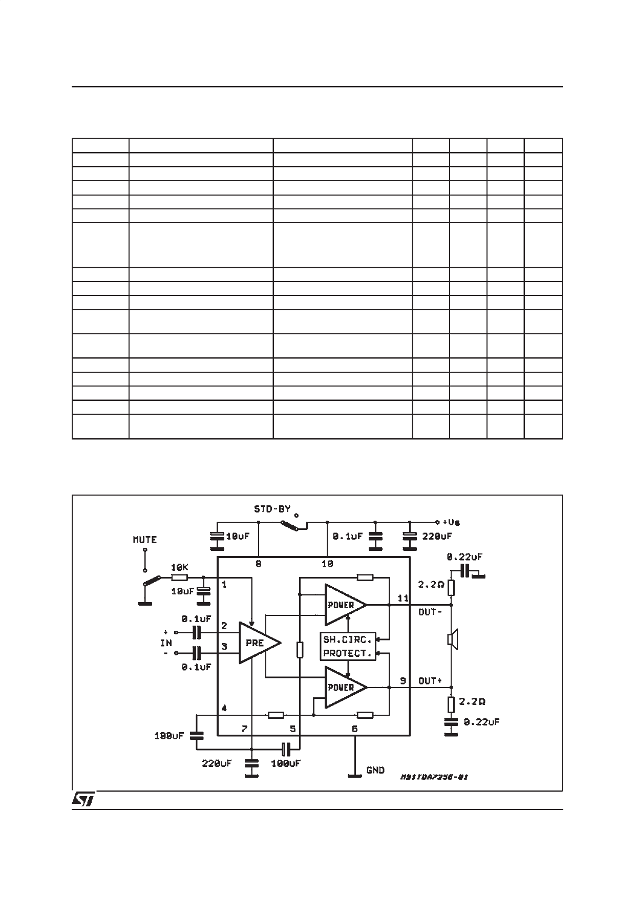
Figure 1: Test and Application Circuit
3/10
Share Link: 