M36W432BG70ZA1 データシートの表示(PDF) - STMicroelectronics
部品番号
コンポーネント説明
メーカー
M36W432BG70ZA1
STMicroelectronics

M36W432BG70ZA1 Datasheet PDF : 66 Pages
| |||
M36W432TG, M36W432BG
SUMMARY DESCRIPTION
The M36W432TG is a low voltage Multiple Memo-
ry Product which combines two memory devices;
a 32 Mbit boot block Flash memory and a 4 Mbit
SRAM. Recommended operating conditions do
not allow both the Flash and SRAM devices to be
active at the same time.
The memory is offered in a Stacked LFBGA66
(12x8mm, 8x8 active ball array, 0.8 mm pitch)
package and is supplied with all the bits erased
(set to ‘1’).
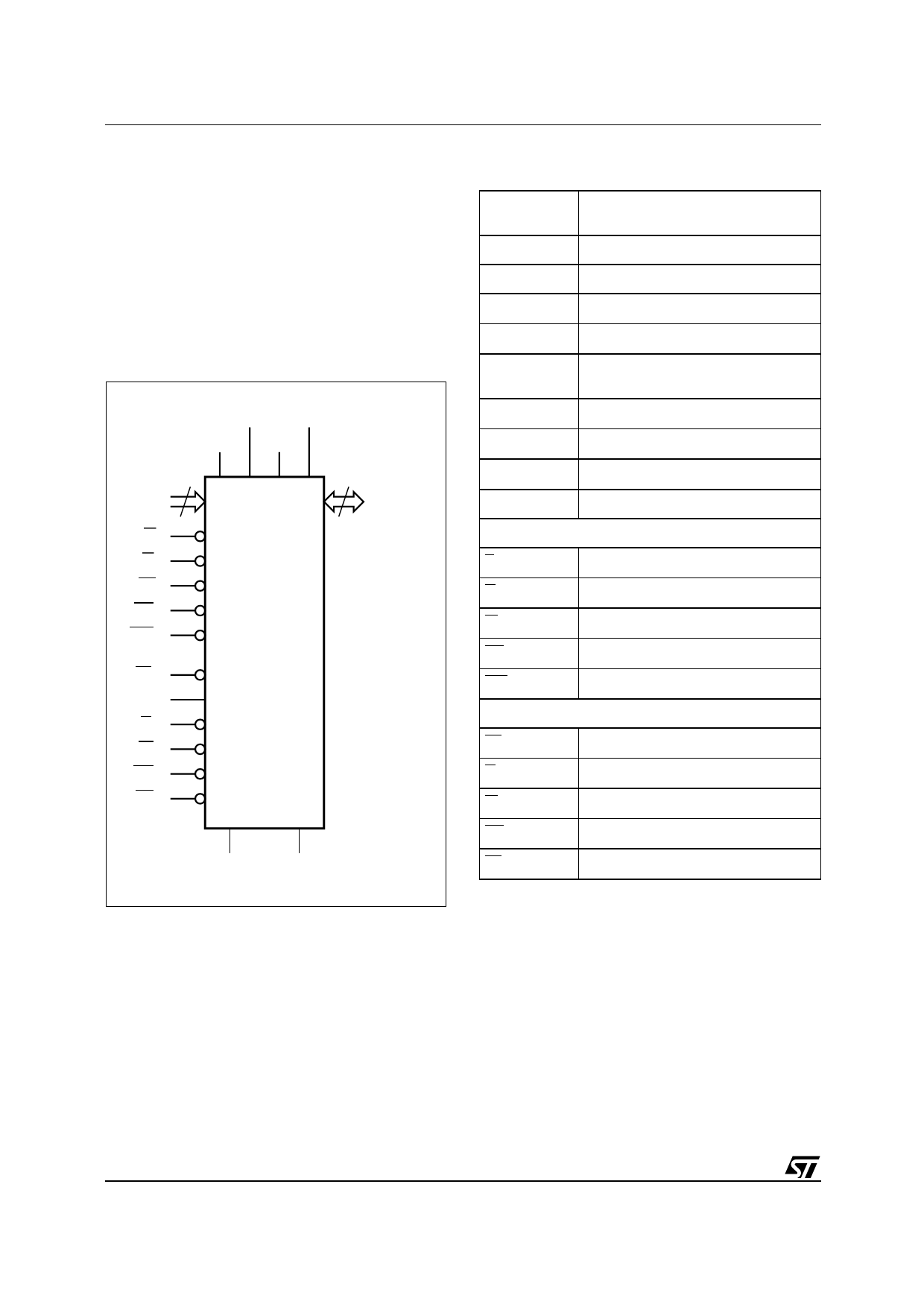
Figure 2. Logic Diagram
VDDQF VDDS
VDDF VPPF
21
A0-A20
16
DQ0-DQ15
EF
GF
WF
RPF
WPF
E1S
E2S
GS
WS
UBS
LBS
M36W432TG
M36W432BG
VSSF
VSSS
AI07925
Table 1. Signal Names
A0-A17
Address Inputs common to the Flash
and SRAM chips
A18-A20
Address Inputs for Flash Chip only
DQ0-DQ15 Data Input/Output
VDDF
Flash Power Supply
VDDQF
Flash Power Supply for I/O Buffers
VPPF
Flash Optional Supply Voltage for Fast
Program & Erase
VSSF
Flash Ground
VDDS
SRAM Power Supply
VSSS
SRAM Ground
NC
Not Connected Internally
Flash control functions
EF
Chip Enable input
GF
Output Enable input
WF
Write Enable input
RPF
Reset input
WPF
Write Protect input
SRAM control functions
E1S, E2S
Chip Enable inputs
GS
Output Enable input
WS
Write Enable input
UBS
Upper Byte Enable input
LBS
Lower Byte Enable input
6/66
Share Link: