MAX496CSE データシートの表示(PDF) - Maxim Integrated
部品番号
コンポーネント説明
メーカー
MAX496CSE Datasheet PDF : 12 Pages
| |||
375MHz Quad Closed-Loop
Video Buffers, AV = +1 and +2
_____________________Pin Description
PIN NAME
1, 3,
5, 7
GND
2
IN0
4
IN1
6
IN2
8
IN3
9, 15
VCC
10
OUT3
11, 13
VEE
12
OUT2
14
OUT1
16
OUT0
FUNCTION
Ground. All ground pins are internally
connected. Connect all ground pins
externally to minimize the ground
impedance.
Channel 0 Input
Channel 1 Input
Channel 2 Input
Channel 3 Input
Positive Power Supply. Connect to +5V.
VCC pins are internally connected.
Connect both pins to +5V externally to
minimize the supply impedance.
Channel 3 Output
Negative power supply. Connect to -5V.
VEE pins are internally connected.
Connect both pins to -5V externally to
minimize the supply impedance.
Channel 2 Output
Channel 1 Output
Channel 0 Output
_______________Detailed Description
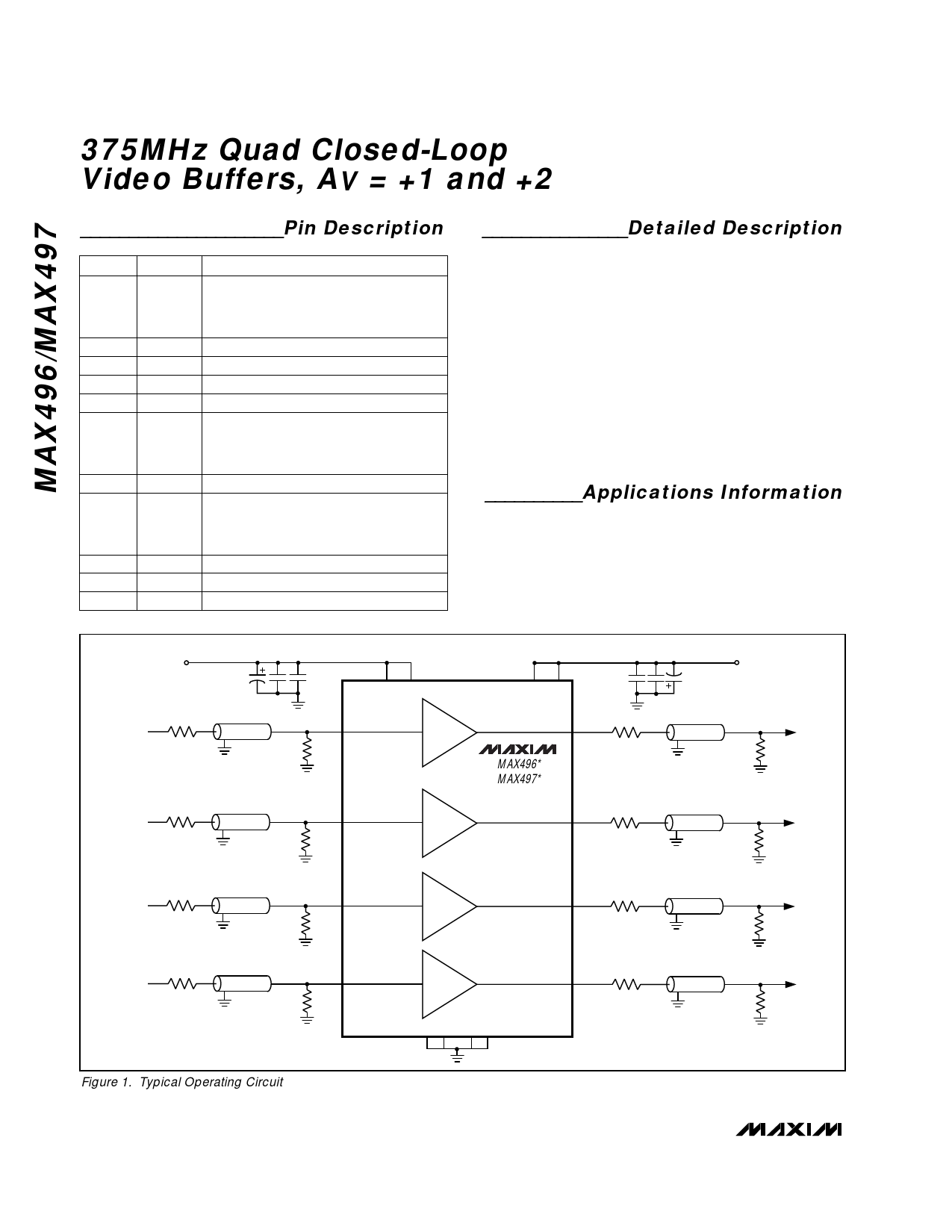
The MAX496/MAX497 are quad, high-speed, closed-loop
voltage-feedback video amplifiers with fixed gain settings
of +1 and +2, respectively (Figure 1). These amplifiers
use a unique two-stage voltage-feedback architecture
that combines the benefits of conventional voltage-feed-
back and current-mode-feedback topologies. They
achieve wide bandwidths and high slew rates while main-
taining precision. A resistively loaded first stage provides
low input-referred noise even with low supply currents of
8mA per amplifier. The above features, along with the
ability to drive 50Ω or 75Ω back-terminated cables to
±2.8V and low differential phase and gain errors, make
these amplifiers ideal for the most demanding component
and composite video applications.
__________Applications Information
The feedback elements of the MAX496/MAX497 are
included internally in the device to set the closed-loop
gain to AV = +1 and AV = +2, respectively. Closing the
loop internally on the chip minimizes problems associ-
ated with the board and package parasitics influencing
the amplifier’s frequency response.
VCC
+5V
0.10µF
10µF
0.10µF
9 15
75Ω
75Ω CABLE
RED
75Ω
2 IN0
75Ω
GREEN
75Ω CABLE
75Ω
4 IN1
AV = *
11 13
0.10µF
0.10µF
10µF
VEE
-5V
OUT0 16
75Ω
75Ω CABLE
75Ω
MAX496*
MAX497*
OUT1 14
75Ω
75Ω CABLE
75Ω
75Ω
BLUE
75Ω CABLE
75Ω
6 IN2
AV = *
OUT2 12
75Ω
75Ω CABLE
75Ω
75Ω
SYNC
75Ω CABLE
75Ω
*AV = +1 (MAX496)
*AV = +2 (MAX497)
Figure 1. Typical Operating Circuit
8 IN3
AV = *
OUT3 10
75Ω
75Ω CABLE
75Ω
GND
3
57
8 _______________________________________________________________________________________
Share Link: 