LA7256 データシートの表示(PDF) - SANYO -> Panasonic
部品番号
コンポーネント説明
メーカー
LA7256 Datasheet PDF : 9 Pages
| |||
LA7256
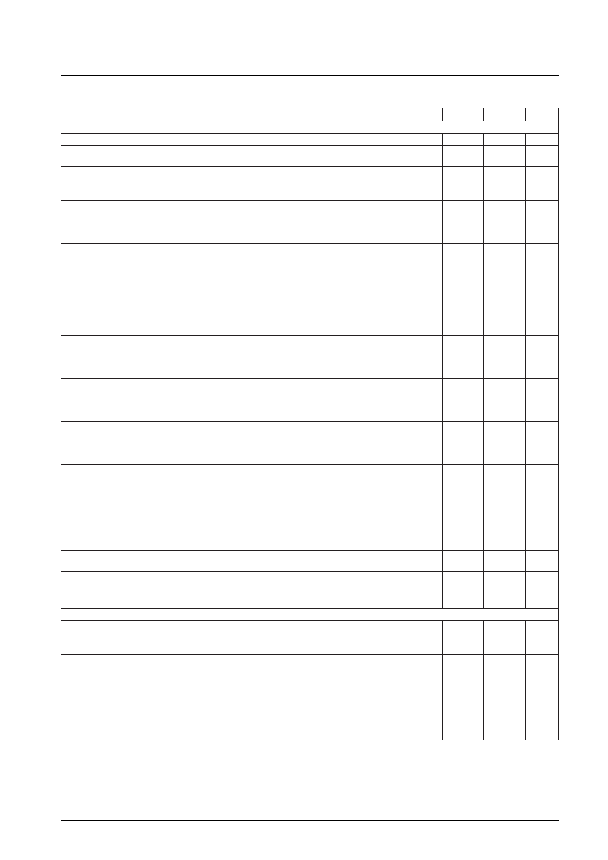
Operating Characteristics at Ta = 25°C, VCC = 5 V, in the specified test circuit
Parameter
Symbol
Conditions
min
typ
[Playback Mode]
Circuit current
Voltage gain, CH1
ICCP
GVP1
No input: the pin 14 influx current
Pin 20 input = 100 µVp-p, f = 1.5 MHz, pin 1 = low:
measure the pin 3 output.
13
18
72.5
75.5
Voltage gain, CH2
GVP2
Pin 17 input = 100 µVp-p, f = 1.5 MHz, pin 1 = high:
measure the pin 3 output.
72.5
75.5
Voltage gain difference
EP gain emphasis
∆GVP
∆GEP
GVP1 – GVP2
Pin 20 input = 100 µVp-p, f = 1.5 MHz, pin 1 = low:
the ratio of the pin 3 outputs when pin 2 is high/low
–2
0
1.7
2.4
Frequency characteristics, CH1
Pin 20 input = 100 µVp-p, pin 1 = low: the difference
fP1
in the levels on pin 3 when f = 2.2 MHz and 1.0 MHz
–3.0
–1.0
Pin 17 input = 100 µVp-p, f = 1.5 MHz, pin 1 = high:
Frequency characteristics, CH2
fP2
the difference in the levels on pin 3 when f = 2.2 MHz
–3.0
–1.0
and 1.0 MHz
Pin 17 input = 0, pin 20 input = 100 µVp-p, f = 1.5 MHz:
Crosstalk CH1 to CH2
CT1 → 2 the difference in the pin 3 output levels when pin 1 goes
–40
from low to high
Pin 20 input = 0, pin 17 output = 100 µVp-p, f = 1.5 MHz:
Crosstalk CH2 to CH1
CT2 → 1 the difference in the pin 3 output levels when pin 1 goes
–40
from high to low
With pin 20 grounded through 0.01 µF and 1 Ω,
Equivalent input noise voltage CH1
VNP1
pin 1 = low: the pin 3 noise in input equivalent*1
0.8
With pin 17 grounded through 0.01 µF and 1 Ω,
Equivalent input noise voltage CH2
VNP2
pin 1 = high: the pin 3 noise in input equivalent*1
0.8
Pin 20 input = 100 µVp-p, f = 1.5 MHz, pin 1 = low:
Second harmonic distortion CH1
2THD1 the second harmonic in the pin 3 output
–50
Pin 17 input = 100 µVp-p, f = 1.5 MHz, pin 1 = high:
Second harmonic distortion CH2
2THD2 the second harmonic in the pin 3 output
–50
With the pin 20 input varying, f = 1.5 MHz, pin 1 = low:
Maximum output voltage CH1
VOMP1 when the pin 3 third harmonic distortion is –30 dB
2.0
Maximum output voltage CH2
With the pin 17 input varying, f = 1.5 MHz, pin 1 = high:
VOMP2 when the pin 3 third harmonic distortion is –30 dB
2.0
Output DC offset 1
Pin 17 and 20 inputs = 0, pin 1 = low, pin 2 = low (SP):
∆VODC1 the difference in the pin 3 DC level when pin 1 goes
–30
0
from low to high
Output DC offset 2
Pin 17 and 20 inputs = 0, pin 1 = low, pin 2 = high (EP):
∆VODC2 the difference in the pin 3 DC level when pin 1 goes
–50
0
from low to high
Head switching: CH1 hold voltage
Head switching: CH2 hold voltage
Playback mode switch
on resistance
VHS1
VHS2
RSW
The pin 1 DC voltage required to operate CH1
The pin 1 DC voltage required to operate CH2
Calculate from the voltage difference on pin 16
when the pin 16 influx current is 1 mA and 2 mA.
0
3.0
4.0
SP hold voltage
EP hold voltage
PB hold voltage
[Record Mode]
V2SP The pin 2 voltage required to hold SP mode
0
V2EP The pin 2 voltage required to hold EP mode
3.0
V5L
The pin 5 voltage required to hold PB mode
0
Circuit current
Output current
ICCR
IOR
No signal, the pin 14 influx current
Pin 9 input = 180 mVp-p, f = 1.5 MHz:
measure the pin 16 output
45
63
48
53
AGC control characteristics 1
Pin 9 input = 90 and 180 mVp-p, f = 1.5 MHz:
∆VAGC1 the ratio of the pin 16 output levels
–0.5
–0.2
Pin 9 input = 360 and 180 mVp-p, f = 1.5 MHz:
AGC control characteristics 2
∆VAGC2 the ratio of the pin 16 output levels
0.2
Cross modulation distortion
0.4 MHz component
CMD04
For a pin 9 input*2, the 0.4 MHz spurious signal
in the pin 16 output current
Cross modulation distortion
0.9 MHz component
CMD09
For a pin 9 input*2, the 0.9 MHz spurious signal
in the pin 16 output current
Note: 1. Measure the input noise voltage after passing the pin 3 output (playback FM output) through a 1.1 MHz low-pass filter.
2. 1.3 MHz (70 mVp-p) + 1.7 MHz (180 mVp-p)
max
Unit
23
mA
78.5
dB
78.5
dB
2
dB
3.1
dB
0
dB
0
dB
–35
dB
–35
dB
1.0
µVrms
1.0
µVrms
–40
dB
–40
dB
Vp-p
Vp-p
+30
mV
+50
mV
1.0
V
VCC
V
6.0
Ω
1.0
V
VCC
V
1.0
V
81
mA
58
mAp-p
dB
0.5
dB
–40
dB
–40
dB
Continued on next page.
No. 4896-2/9
Share Link: 