ISL88705(2006) гГЗгГЉгВњгВЈгГЉгГИгБЃи°®з§ЇпЉИPDFпЉЙ - Intersil
йГ®еУБзХ™еПЈ
гВ≥гГ≥гГЭгГЉгГНгГ≥гГИи™ђжШО
гГ°гГЉгВЂгГЉ
ISL88705
(Rev.:2006)
(Rev.:2006)
Intersil

ISL88705 Datasheet PDF : 14 Pages
| |||
ISL88705, ISL88706, ISL88707, ISL88708, 8SL88716, ISL88813
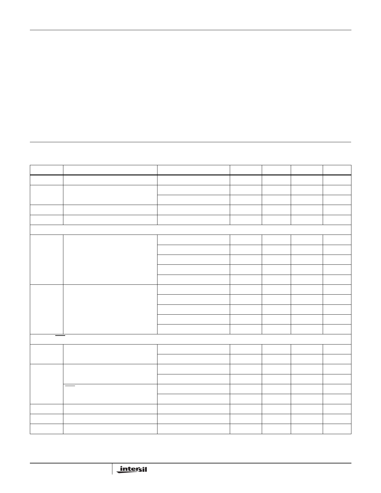
Absolute Maximum Ratings
Temperature Under Bias . . . . . . . . . . . . . . . . . . . . .-40°C to +125°C
Storage Temperature . . . . . . . . . . . . . . . . . . . . . . .-65°C to +150°C
Voltage on any Pin with Respect to GND . . . . . . . . . . . -1.0V to +7V
DC Output Current . . . . . . . . . . . . . . . . . . . . . . . . . . . . . . . . . . . 5mA
Lead Temperature (Soldering, 10s) . . . . . . . . . . . . . . . . . . . . +300°C
Recommended Operating Conditions
Temperature Range (Industrial) . . . . . . . . . . . . . . . . .-40°C to +85°C
Thermal Information
Thermal Resistance (Typical, Note 3)
PDIP Package* (4-layer test board) . . . . . . . . . . . . .
SOIC Package (4-layer test board) . . . . . . . . . . . . .
ќЄJA (¬∞C/W)
83
110
*Pb-free PDIPs can be used for through hole wave solder processing
only. They are not intended for use in Reflow solder processing
applications.
CAUTION: Absolute Maximum Ratings indicate limits beyond which permanent damage to the device and impaired reliability may occur. These are stress ratings
provided for information only and functional operation of the device at these or any other conditions beyond those indicated in the operational sections of this
specification are not implied.
For guaranteed specifications and test conditions, see Electrical Specifications. The guaranteed specifications apply only for the test conditions listed. Some
performance characteristics may degrade when the device is not operated under the listed test conditions.
NOTE:
3. ќЄJA is measured with the component mounted on a high effective thermal conductivity test board in free air. See Tech Brief TB379 for details.
Electrical Specifications Over the recommended operating conditions unless otherwise specified.
SYMBOL
PARAMETER
CONDITIONS
MIN
TYP
VDD
IDD
Supply Voltage Range
ILI
Input Leakage Current (PFI)
ILO
Output Leakage Current
VOLTAGE THRESHOLDS
VDD = 5V, WDT Inactive
VDD = 3V, WDT Inactive
2.0
10
8
VTH1
Fixed VDD Voltage Trip Point
4.556
4.301
4.640
4.380
3.034
3.090
2.867
2.920
2.583
2.630
VTH1HYST Hysteresis at VTH1 Input
VTH1 = 4.64V
46
Temperature = +25°C
VTH1 = 4.38V
44
VTH1 = 3.09V
37
VTH1 = 2.92V
29
VTH1 = 2.63V
31
RST AND RST
VOL
Reset Output Voltage Low
VOH
RST Output Voltage High
RST Output Voltage High
tRPD
tPOR
CLOAD
VTH to Reset Asserted Delay
POR Time-Out Delay
Load Capacitance on Reset Pins
VDD вЙ• 3.3V, Sinking 2.5mA
VDD < 3.3V, Sinking 1.5mA
VDD вЙ• 3.3V, Sourcing 2.5mA
VDD < 3.3V, Sourcing 1.5mA
VDD вЙ• 3.3V, Sourcing 0.8mA
VDD < 3.3V, Sourcing 0.5mA
CPOR is open
VDD-0.6
VDD-0.6
VDD-0.6
VDD-0.6
140
0.05
0.05
VDD-0.4
VDD-0.4
VDD-0.4
VDD-0.4
45
200
5
MAX
5.5
19
10
100
100
4.724
4.459
3.146
2.973
2.677
0.40
0.40
260
UNITS
V
µA
µA
nA
nA
V
V
V
V
V
mV
mV
mV
mV
mV
V
V
V
V
V
V
µs
ms
pF
5
FN8092.3
December 6, 2006
Share Link: