BD3501FVM(2008) データシートの表示(PDF) - ROHM Semiconductor
部品番号
コンポーネント説明
メーカー
BD3501FVM
(Rev.:2008)
(Rev.:2008)
ROHM Semiconductor

BD3501FVM Datasheet PDF : 17 Pages
| |||
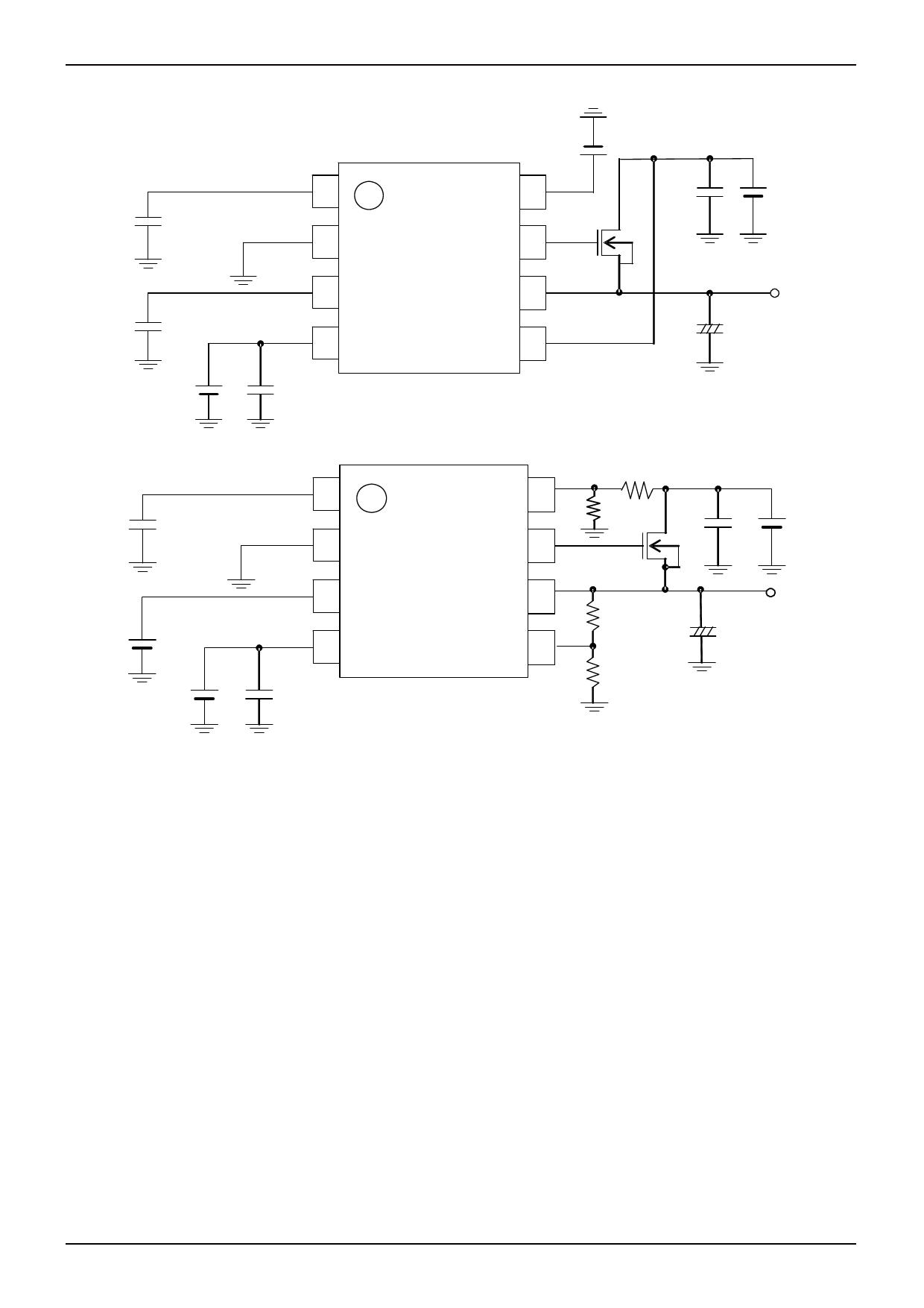
●APPLICATION CIRCUIT
C3
C2
Vcc
1
2
3
4
C1
C3
Ven
Vcc
1
2
3
4
C1
Ven
8
C4
VIN
7
6
C5 +
5
R2’
8
R1’
7
VIN
C2
6
R2
C4 +
5
R1
●Directions for pattern layout of PCB
・Because a VIN input capacitor causes impedance to drop, mount it as close to the VIN terminal as possible and use thick
wiring patterns. In the event that it causes the wire to come in contact with the inner-layer ground plane, use a plurality of
through holes.
・Because the NRCS terminal is analog I/O, take care to noise. In particular, high-frequency noise of GND may cause IC
maloperation through capacitors. It is recommended to connect GND of NRCS capacitor to IC GND terminal at one point.
・The VFB terminal is an output voltage sense line. Effects of wiring impedance can be ignored by sensing the output voltage
from the load side, but increased sense wiring causes VFB to be susceptible to noise, to which care must be taken.
・Because the GND terminal is GND to be used in analog circuit inside BD3501/02/04FVM, connect it at one point to inner-layer
GND of substrate by as short pattern as possible. Arrange a bypass capacitor across VCC and GND as close as possible so
that a loop can be minimized.
・The G terminal is a terminal for gate drive. If long wiring is inevitable, increase the pattern width and lower impedance.
・Heat generated in the output transistor can be calculated by:
(VIN - VOUT) × Io(Max)
Design heat generation not to exceed the guarantee temperature of transistor.
・Connect the output capacitor with thick short wiring so that the impedance is lowered. Connect capacitor GND to inner-layer
GND plane by a plurality of through holes.
10/16
Share Link: