BD3500FVM-TR(2008) データシートの表示(PDF) - ROHM Semiconductor
部品番号
コンポーネント説明
メーカー
BD3500FVM-TR
(Rev.:2008)
(Rev.:2008)
ROHM Semiconductor

BD3500FVM-TR Datasheet PDF : 17 Pages
| |||
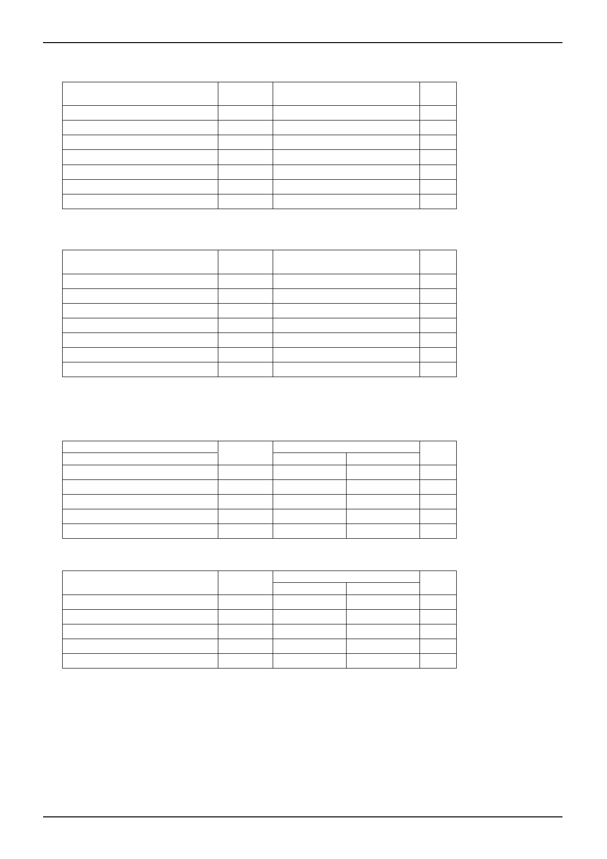
●ABSOLUTE MAXIMUM RATINGS (Ta=25℃)
◎BD3500/01/02FVM
Parameter
Input Voltage
Symbol
Limit
Unit
VCC
7 *1
V
Drain Voltage (VIN)
VIN
7
V
Enable Input Voltage
Power Dissipation
Ven
7
V
Pd
437.5 *2
mW
Operating Temperature Range
Topr
-10~+100
℃
Storage Temperature Range
Tstg
-55~+150
℃
Maximum Junction Temperature
Tjmax
+150
℃
*1 However, not exceeding Pd.
*2 Pd derating at 3.5mW/℃ for temperature above Ta=25℃
◎BD3504FVM
Parameter
Supply Voltage
Symbol
Limit
Unit
VCC
7 *3
V
Drain Voltage
VD
7
V
Enable Input Voltage
Power dissipation
Ven
7
V
Pd
437.5 *4
mW
Operating temperature range
Topr
-10~+100
℃
Storage temperature range
Tstg
-55~+150
℃
Maximum Junction Temperature
Tjmax
+150
℃
*3 However, not exceeding Pd.
*4 Pd derating at 3.5mW/℃ for temperature above Ta=25℃
●RECOMMENDED OPERATING CONDITIONS
◎BD3500/01/02FVM
Parameter
Symbol
MIN
MAX
Unit
Supply Voltage
VCC
4.5
5.5
V
Drain Voltage(VIN)
VIN
Vo×1.15
5.5
V
Enable Input Voltage
Ven
-0.3
5.5
V
Capacitor on NRCS Terminal
CNRCS
0.001
1
uF
Capacitor on SCP Terminal
CSCP
0.001
1
uF
★ No radiation-resistant design is adopted for the present product.
◎BD3504FVM
Parameter
Supply Voltage
Drain Voltage
Enable Input Voltage
Capacitor in NRCS pin
Output Voltage
Symbol
MIN
MAX
Unit
VCC
4.5
5.5
V
VD
0.65
5.5
V
Ven
-0.3
5.5
V
CNRCS
0.001
1
uF
VOUT
0.65
2.5
V
★ No radiation-resistant design is adopted for the present product.
2/16
Share Link: