ICPL2533 データシートの表示(PDF) - Unspecified
部品番号
コンポーネント説明
メーカー
ICPL2533 Datasheet PDF : 4 Pages
| |||
SWITCHING SPECIFICATIONS AT TA = 25°C ( VCC = 5V Unless otherwise noted )
PARAMETER
SYM DEVICE MIN TYP MAX UNITS TEST CONDITION
Propagation Delay Time
tPHL
to Logic Low at Output ( fig 1 )
0.8 1.5 µs
0.3 1.5 µs
IF = 8mA,RL= 7.5kΩ
(note 10 )
I
F
=
16mA,R =
L
4.7kΩ,
(note11 )
Propagation Delay Time
t
PLH
to Logic High at Output ( fig 1 )
1.0 2.5 µs
1.1 2.5 µs
IF = 8mA,RL= 7.5kΩ,
(note 10 )
I
F
=
16mA,R =
L
4.7kΩ,
(note11 )
Common Mode Transient
Immunity at Logic High
Level Output ( fig 2 )
CM
H
1000
1000
V/µs
V/µs
IF = 0mA, VCM = 10VPP
R=
L
7.5kΩ,(note9,10
)
IF = 0mA, VCM = 10VPP
RL = 4.7kΩ,(note9,11 )
Common Mode Transient
Immunity at Logic Low
CM
L
Level Output ( fig 2 )
-1000
V/µs
-1000
V/µs
I = 8mA,V = 10V
F
CM
PP
RL = 7.5kΩ,(note9,10 )
IF = 16mA,VCM= 10VPP
R
L
=
1.9kΩ,(note9,11
)
NOTES:-
1. Derate linearly above 70oC free air temperature at a rate of 0.8 mA/°C.
2. Derate linearly above 70oC free air temperature at a rate of 1.6 mA/°C.
3. Derate linearly above 70oC free air temperature at a rate of 0.9 mW/°C.
4. Derate linearly above 70oC free air temperature at a rate of 1.0 mW/°C.
5. Each channel .
6. CURRENT TRANSFER RATIO is defined as the ratio of output collector current,I , to the forward LED
O
input current, IF times 100%.
7. Device considered a two-terminal device: pins 1,2,3,and 4 shorted together and pins 5,6,7,and 8 shorted
together.
8. Measured between pins 1 and 2 shorted together, and pins 3 and 4 shorted together.
9. Common mode transient immunity in Logic High level is the maximum tolerable (positive) dVcm/dt on
the leading edge of the common mode pulse VCM to assure that the output will remain in a Logic High
state (i.e. V > 2.0V). Common mode transient immunity in Logic Low level is the maximum tolerable
O
(negative) dVcm/dt on the trailing edge of the common mode pulse signal, V to assure that the output
CM
will remain in Logic Low state (i.e. VO< 0.8V).
10. The 7.5kΩ load represents 1 LSTTL unit load of 0.36mA and a 20kΩ pull-up resistor.
11. The 4.7kΩ load represents 1 LSTTL unit load of 0.36mA and a 8.2kΩ pull-up resistor.
12. The 2500 V / 1minute capability is validated by a factory 3.1k V / 1 second dielectric test.
RMS
RMS
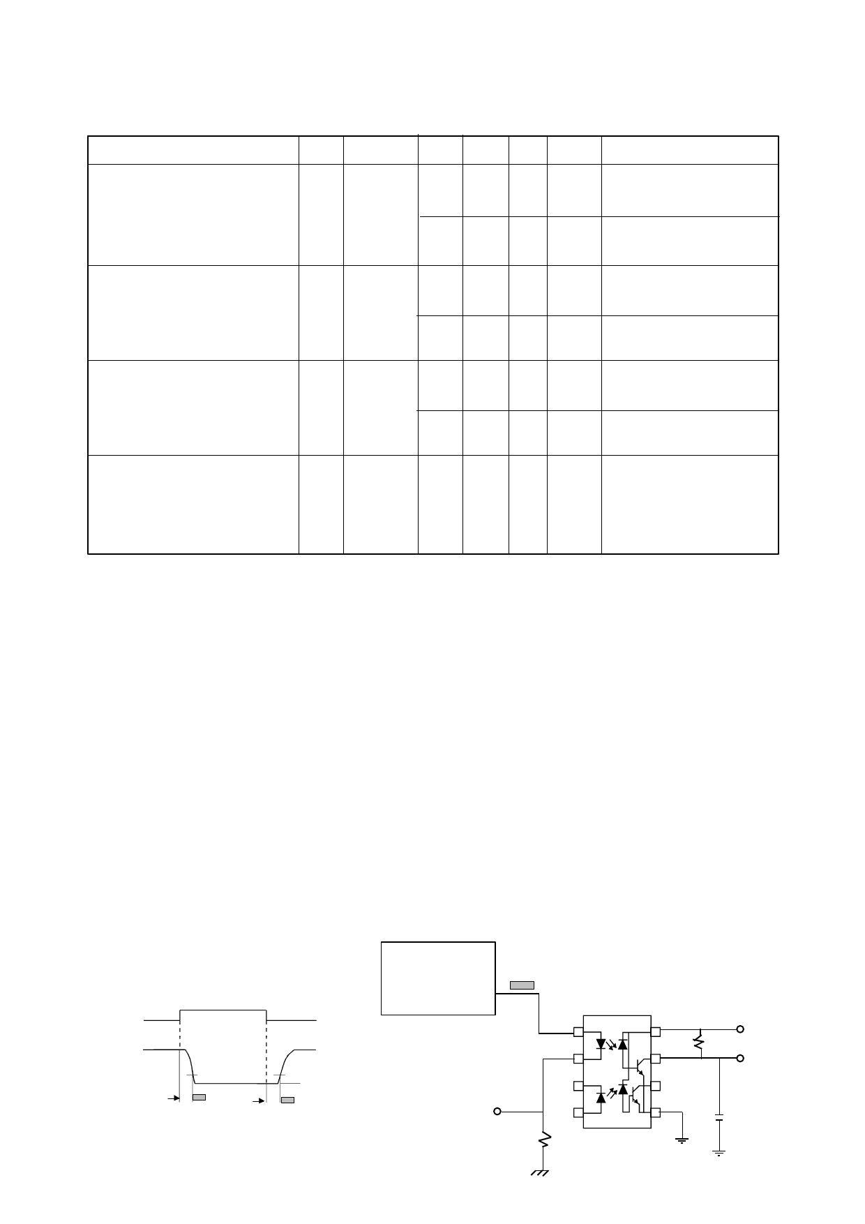
FIG.1 SWITCHING TEST CIRCUIT
IF
0
V
O
t
PHL
1.3V
t
PLH
5V
1.3V
VOL
PULSE
GENERATOR
ZO = 50Ω
IF
t = 5ns
r
10% Duty Cycle
1
1/f < 100µs
2
3
IF Monitor
4
100Ω
8
5V
7
R
L
V
O
6
5
C = 15pF
L
7/12/00
DB91038-AAS/A3
Share Link: 