DS3510TR データシートの表示(PDF) - Maxim Integrated
部品番号
コンポーネント説明
メーカー
DS3510TR Datasheet PDF : 17 Pages
| |||
I2C Gamma and VCOM Buffer with EEPROM
NONVOLATILE MEMORY CHARACTERISTICS
(VCC = +2.7V to +5.5V.)
PARAMETER
EEPROM Write Cycles
EEPROM Write Cycles
SYMBOL
TA = +70°C
TA = +25°C
CONDITIONS
MIN
50,000
200,000
MAX
UNITS
Writes
Writes
Note 1: All voltages are referenced to ground. Currents entering the IC are specified positive and currents exiting the IC are
negative.
Note 2: IDD supply current is specified with VDD = 15.0V and no load on VCOM or GM1–10 outputs.
Note 3: Specified with the VCOM and gamma bias currents set to 100%.
Note 4: ICC is specified with the following conditions: SCL = 400kHz, SDA = VCC = 5.5V, and VCOM and GM1–10 floating.
Note 5: ICCQ is specified with the following conditions: SCL = SDA = VCC = 5.5V, and VCOM and GM1–10 floating.
Note 6: IDDQ is specified with the following conditions: SCL = SDA = VCC = 5.5V and VCOM and GM1–10 floating.
Note 7: Guaranteed by design.
Note 8: Integral nonlinearity is the deviation of a measured value from the expected values at each particular setting. Expected
value is calculated by connecting a straight line from the measured minimum setting to the measured maximum setting.
INL = [V(RW)i - (V(RW)0]/LSB(measured) - i, for i = 0...255.
Note 9: Differential nonlinearity is the deviation of the step size change between two LSB settings from the expected step size. The
expected LSB step size is the slope of the straight line from measured minimum position to measured maximum position.
DNL = [V(RW)i+1 - (V(RW)i]/LSB(measured) - 1, for i = 0...254.
Note 10: Tested at VRL = VRH = 6.5V/7.5V/8.5V, GLL = GLM = 0.5V/6.5V/8.5V/14.5V, GHM = GHH = 0.5V/6.5V/8.5V/14.5V.
Note 11: EEPROM data is assumed already settled at input of Latch B. LD transitions after EEPROM byte has been selected.
Note 12: Rising transition from 5V to 10V; falling transition from 10V to 5V.
Note 13: I2C interface timing shown is for fast-mode (400kHz) operation. This device is also backward-compatible with I2C
standard mode timing.
Note 14: CB—total capacitance of one bus line in picofarads.
Note 15: EEPROM write time begins after a STOP condition occurs.
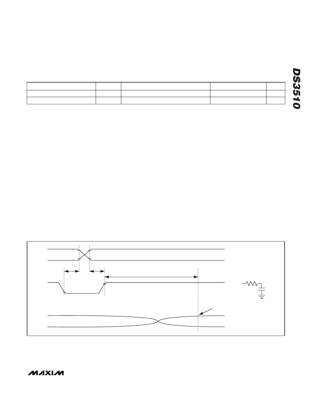
Note 16: Pulses narrower than max are suppressed.
S0/S1
tHD
LD
VIL
VIH
VIL
tSU
VIH
VCOM
Figure 1. VCOM Settling Timing Diagram
tSET-V
2Ω
VCOM
100nF
0.1% SETTLED
_______________________________________________________________________________________ 5
Share Link: 