MLCE17E3 データシートの表示(PDF) - Microsemi Corporation
部品番号
コンポーネント説明
メーカー
MLCE17E3 Datasheet PDF : 5 Pages
| |||
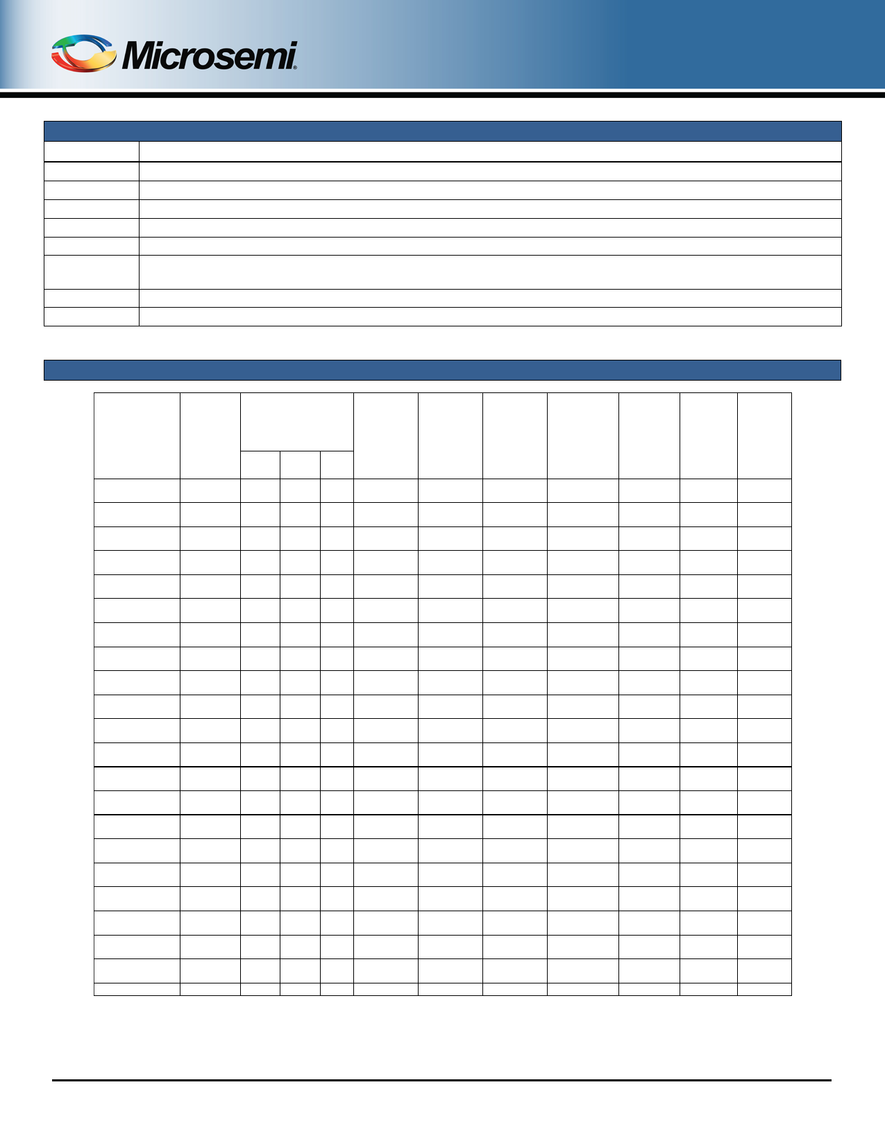
MLCE6.5 – MLCE170A
Symbol
I (BR)
ID
IF
I PP
P PP
VC
V (BR)
VWM
SYMBOLS & DEFINITIONS
Definition
Breakdown Current: The current used for measuring breakdown voltage V(BR).
Standby Current: The current at the rated standoff voltage VWM.
Forward Current: The forward current dc value, no alternating component.
Peak Impulse Current: The peak current during the impulse.
Peak Pulse Power: The peak power dissipation resulting from the peak impulse current IPP.
Clamping Voltage: The maximum clamping voltage at specified IPP (peak pulse current) at the specified pulse
conditions.
Minimum Breakdown Voltage: The minimum voltage the device will exhibit at a specified current.
Working Standoff Voltage: The maximum peak voltage that can be applied over the operating temperature range.
ELECTRICAL CHARACTERISTICS @ 25 ºC unless otherwise stated
MICROSEMI
Part Number
MLCE6.5A
MLCE7.0A
MLCE7.5A
MLCE8.0A
MLCE8.5A
MLCE9.0A
MLCE10A
MLCE11A
MLCE12A
MLCE13A
MLCE14A
MLCE15A
MLCE16A
MLCE17A
MLCE18A
MLCE20A
MLCE22A
MLCE24A
MLCE26A
MLCE28A
MLCE30A
MLCE33A
MLCE36A
MLCE40A
MLCE43A
MLCE45A
MLCE48A
MLCE51A
MLCE54A
MLCE58A
MLCE60A
MLCE64A
MLCE70A
MLCE75A
MLCE80A
MLCE90A
MLCE100A
MLCE110A
MLCE120A
MLCE130A
MLCE150A
MLCE160A
MLCE170A
Working
Stand-Off
Voltage
V WM
(Note 1)
Volts
6.5
7.0
7.5
8.0
8.5
9.0
10
11
12
13
14
15
16
17
18
20
22
24
26
28
30
33
36
40
43
45
48
51
54
58
60
64
70
75
80
90
100
110
120
130
150
160
170
Breakdown Voltage
V (BR) @ I (BR)
Volts
MIN MAX mA
7.22 7.98 10
7.78 8.60 10
8.33 10.2 10
8.89 9.83 1
9.44 10.4 1
10.0 11.1 1
11.1 12.3 1
12.2 13.5 1
13.3 14.7 1
14.4 15.9 1
15.6 17.2 1
16.7 18.5 1
17.8 19.7 1
18.9 20.9 1
20.0 22.1 1
22.2 24.5 1
24.4 26.9 1
26.7 29.5 1
28.9 31.9 1
31.1 34.4 1
33.3 36.8 1
36.7 40.6 1
40.0 44.2 1
44.4 49.1 1
47.8 52.8 1
50.0 55.3 1
53.3 58.9 1
56.7 62.7 1
60.0 66.3 1
64.4 71.2 1
66.7 73.7 1
71.1 78.6 1
77.8 86.0 1
83.3 92.1 1
88.7 98.0 1
100 111
1
111 123
1
122 135
1
133 147
1
144 159
1
167 185
1
178 197
1
189 209
1
Maximum
Stanby
Current
I D @ V WM
µA
1000
500
250
100
50
10
5
5
5
5
5
5
5
5
5
5
5
5
5
5
5
5
5
5
5
5
5
5
5
5
5
5
5
5
5
5
5
5
5
5
5
5
5
Maximum
Clamping
Voltage
V C @ I PP
Maximum
Peak Pulse
Current
I PP
Maximum
Capacitance
C @ 0 Volts,
f = 1 MHz
Working
Inverse
Blocking
Voltage
V WIB
Volts
Amps
pF
Volts
11.2
100
100
75
12.0
100
100
75
12.9
100
100
75
13.6
100
100
75
14.4
100
100
75
15.4
97
100
75
17.0
88
100
75
18.2
82
100
75
19.9
75
100
75
21.5
70
100
75
23.2
65
100
75
24.4
61
100
75
26.0
57
100
75
27.6
54
100
75
29.2
51
100
75
32.4
46
100
75
35.5
42
100
75
38.9
39
100
75
42.1
36
100
75
45.5
33
100
75
48.4
31
100
75
53.3
28.1
100
75
58.1
25.8
100
75
64.5
23.3
100
75
69.4
21.6
100
150
72.7
20.6
100
150
77.4
19.4
100
150
82.4
18.2
100
150
87.1
17.2
100
150
93.6
16.0
100
150
96.8
15.5
90
150
103
14.6
90
150
113
13.3
90
150
121
12.4
90
150
129
11.6
90
150
146
10.3
90
300
162
9.3
90
300
178
8.4
90
300
193
7.8
90
300
209
7.2
90
300
243
6.2
90
300
259
5.8
90
300
275
5.4
90
300
Inverse
Blocking
Leakage
Current
I IB
Peak
Inverse
Blocking
Voltage
V PIB
µA
Volts
10
100
10
100
10
100
10
100
10
100
10
100
10
100
10
100
10
100
10
100
10
100
10
100
10
100
10
100
10
100
10
100
10
100
10
100
10
100
10
100
10
100
10
100
10
100
10
100
10
200
10
200
10
200
10
200
10
200
10
200
10
200
10
200
10
200
10
200
10
200
10
200
10
200
10
400
10
400
10
400
10
400
10
400
10
400
NOTE 1: TVS are normally selected according to the reverse “standoff voltage” (VWM) which should be equal to or greater than the dc or continuous
peak operating voltage level.
RF01009, Rev. B (5/7/13)
©2013 Microsemi Corporation
Page 3 of 5
Share Link: 