BA9756FS データシートの表示(PDF) - ROHM Semiconductor
部品番号
コンポーネント説明
メーカー
BA9756FS Datasheet PDF : 9 Pages
| |||
Multimedia ICs
BA9756FS
!Pin descriptions
Pin No.
Pin name
Function
1
ERRIN
(error amplifier + input)
This is the recovery voltage input pin.
2
AGC
Capacitance should be determined taking into consideration the linearity at the minimum
(constant for AGC) oscillation frequency, and the response time when the frequency changes.
3
N.C.
See*1.
4
SAWOUT
(constant for
This is the output pin for optimized sawtooth waves, based on the maximum oscillation
frequency.
fMax120kHz C = 1000pF fMax100kHz C = 1200pF
sawtooth wave)
fMax 80kHz C = 1500pF fMax 60kHz C = 2000pF
5
N.C.
See*1.
6
MMCR
(delay constant for
monostable multivibrator)
A charging resistance of 4.7kΩ or higher should be used.
The threshold level is 4.5V.
7
HDIN
(Hd pulse input)
The threshold level is approximately 2.1V.
8
VREF9
(Ref 9V output)
An output deviation of ± 0.7% is assured through trimming.
9
N.C.
See*1.
10
GND
(Signal GND)
This may be shared with the power GND, but make sure sufficiently stable grounding
is provided.
11
GND
(Power GND)
This may be shared with the signal GND, but make sure sufficiently stable grounding
is provided.
If a voltage of less than GND or higher than VCC is applied because of external back
12
PWMOUT
electromotive force, a protective diode should be inserted (*2).
(PWM output) If the protector circuit and thermal shutdown circuit are tripped, output is fixed at high (VCC)
level.
13
N.C.
See*1.
14
VCC2
(Power VCC)
A decoupling capacitor should be positioned in the vicinity of this pin.
DTC IN
The voltage input to this pin enables restriction of the PWM output duty.
15
(dead time
The duty control is between 0V and 9V, and approximately 0% to 100% is enabled. At 0V,
control input)
however, restrictions apply.
The minimum pulse width for the PWM is 0.85µs (Typ. at 90kHz).
16
(error
ERROUT
amplifier output)
This
is
the
output
pin
for
the
error
amplifier.
17
N.C.
See*1.
18
N.C.
See*1.
19
ERRREF
This is the input pin for the reference voltage.
(error amplifier input)
20
VCC1
A decoupling capacitor should be positioned in the vicinity of this pin.
(signal VCC)
*1 N.C. pin processing
In order to boost the thermal effect of the IC, we recommend connecting this to the GND or to an adjacent pin.
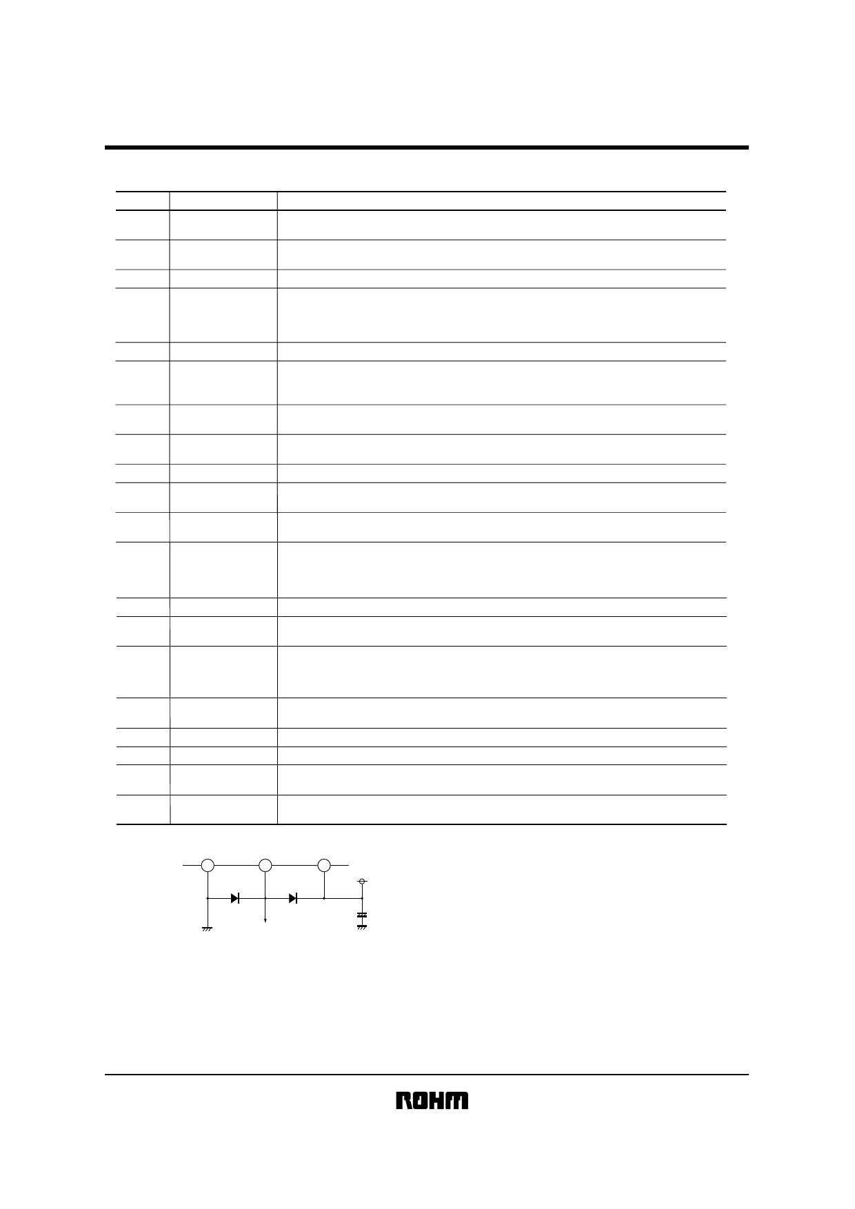
*2
11
12
14
VCC2
+
TO FET gate
Share Link: 