ISPLSI5384VE-80LB272 データシートの表示(PDF) - Lattice Semiconductor
部品番号
コンポーネント説明
メーカー
ISPLSI5384VE-80LB272 Datasheet PDF : 22 Pages
| |||
Specifications ispLSI 5384VE
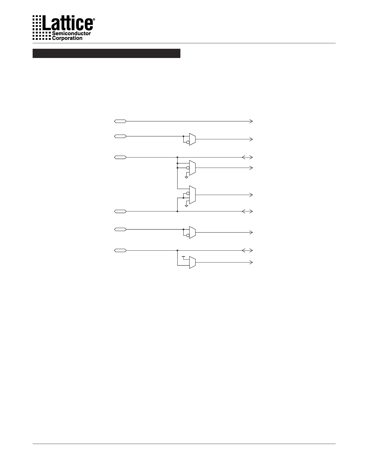
Global Clock Distribution
The ispLSI 5000VE Family has four dedicated clock input
pins: CLK0 - CLK3. CLK0 input is used as the dedicated
master clock that has the lowest internal clock skew with
no clock inversion to maintain the fastest internal clock
speed. The clock inversion is available on the remaining
CLK1 - CLK3 signals. By sharing the pins with the I/O
pins, CLK2 and CLK3 can not only be inverted but are
also available for logic implementation through GRP
signal routing. Figure 5 shows these different clock
distribution options.
Figure 5. ispLSI 5000VE Global Clock Structure
CLK 0
(dedicated pin)
CLK 1
(dedicated pin)
IO/CLK 2
(shared pin)
CLK0
CLK1
to/from GRP
CLK2
IO/CLK 3
(shared pin)
RESET
(dedicated pin)
IO0/TOE
(shared pin)
CLK3
to/from GRP
Global Reset
to/from GRP
TOE
7
Share Link: 