M58CR064DZB データシートの表示(PDF) - STMicroelectronics
部品番号
コンポーネント説明
メーカー
M58CR064DZB Datasheet PDF : 70 Pages
| |||
M58CR064C, M58CR064D, M58CR064P, M58CR064Q
Note: Each device in a system should have
VDD, VDDQ and VPP decoupled with a 0.1µF ce-
ramic capacitor close to the pin (high frequen-
cy, inherently low inductance capacitors
should be as close as possible to the pack-
age). See Figure 9, AC Measurement Load Cir-
cuit. The PCB track widths should be sufficient
to carry the required VPP program and erase
currents.
BUS OPERATIONS
There are six standard bus operations that control
the device. These are Bus Read, Bus Write, Ad-
dress Latch, Output Disable, Standby and Reset.
See Table 3, Bus Operations, for a summary.
Typically glitches of less than 5ns on Chip Enable
or Write Enable are ignored by the memory and do
not affect Bus Write operations.
Bus Read. Bus Read operations are used to out-
put the contents of the Memory Array, the Elec-
tronic Signature, the Status Register and the
Common Flash Interface. Both Chip Enable and
Output Enable must be at VIL in order to perform a
read operation. The Chip Enable input should be
used to enable the device. Output Enable should
be used to gate data onto the output. The data
read depends on the previous command written to
the memory (see Command Interface section).
Refer to the Read AC Waveform figures and Char-
acteristics tables in the DC and AC Parameters
section for details of when the output becomes val-
id.
Bus Write. Bus Write operations write Com-
mands to the memory or latch Input Data to be
programmed. A bus write operation is initiated
when Chip Enable and Write Enable are at VIL with
Output Enable at VIH. Commands, Input Data and
Addresses are latched on the rising edge of Write
Enable or Chip Enable, whichever occurs first. The
addresses can also be latched prior to the write
operation by toggling Latch Enable. In this case
the Latch Enable should be tied to VIH during the
bus write operation.
See Figures 14 and 15, Write AC Waveforms, and
Tables 22 and 23, Write AC Characteristics, for
details of the timing requirements.
Address Latch. Address latch operations input
valid addresses. Both Chip enable and Latch En-
able must be at VIL during address latch opera-
tions. The addresses are latched on the rising
edge of Latch Enable.
Output Disable. The outputs are high imped-
ance when the Output Enable is at VIH.
Standby. Standby disables most of the internal
circuitry allowing a substantial reduction of the cur-
rent consumption. The memory is in stand-by
when Chip Enable and Reset/Power-Down are at
VIH. The power consumption is reduced to the
stand-by level and the outputs are set to high im-
pedance, independently from the Output Enable
or Write Enable inputs. If Chip Enable switches to
VIH during a program or erase operation, the de-
vice enters Standby mode when finished.
Reset. During Reset mode the memory is dese-
lected and the outputs are high impedance. The
memory is in Reset mode when Reset/Power-
Down is at VIL. The power consumption is reduced
to the Standby level, independently from the Chip
Enable, Output Enable or Write Enable inputs. If
Reset is pulled to VSS during a Program or Erase,
this operation is aborted and the memory content
is no longer valid.
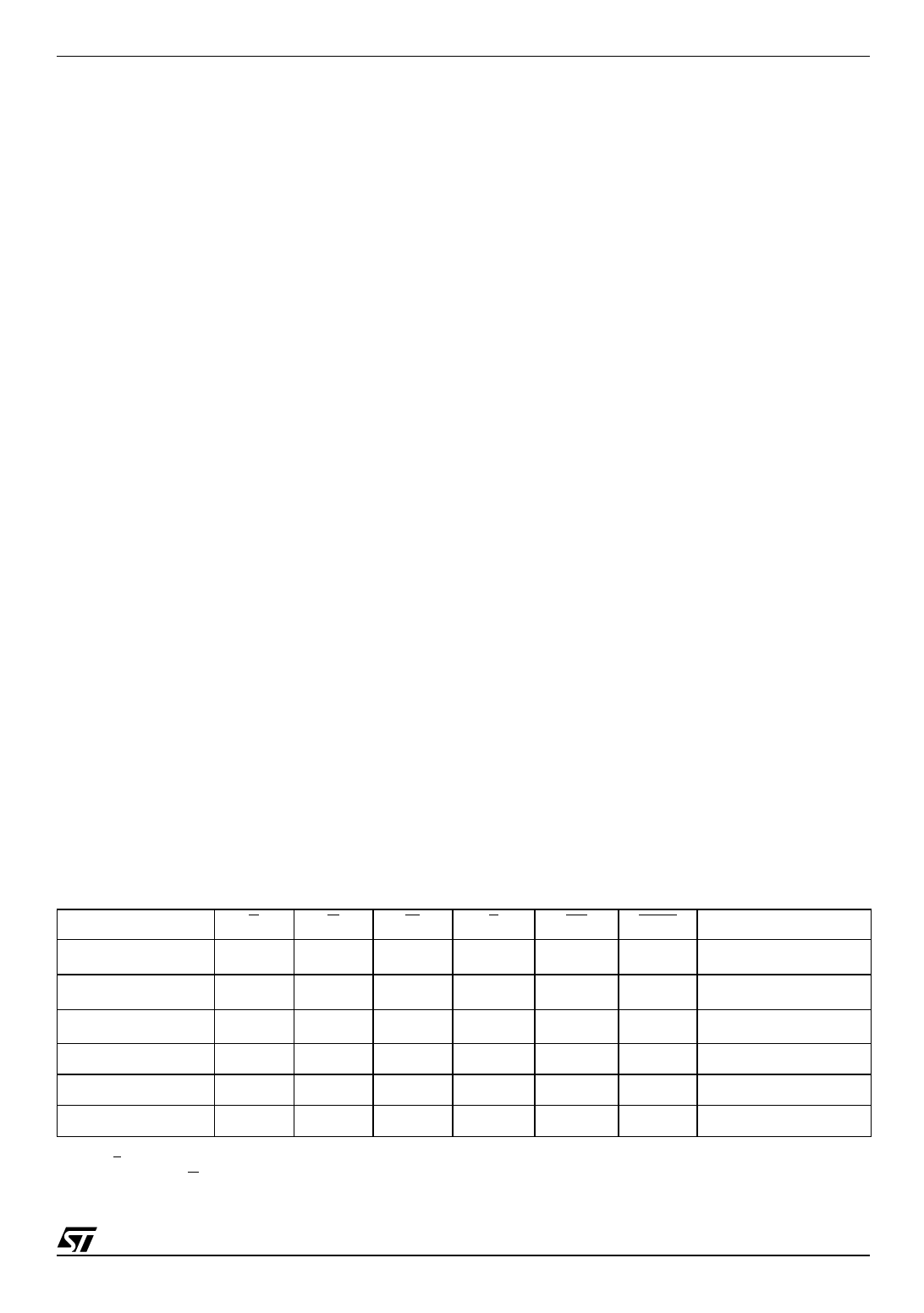
Table 3. Bus Operations
Operation
E
G
W
L
Bus Read
VIL
VIL
VIH
VIL(2)
Bus Write
VIL
VIH
VIL
VIL(2)
Address Latch
VIL
X
VIH
VIL
Output Disable
VIL
VIH
VIH
X
Standby
VIH
X
X
X
Reset
X
X
X
X
Note: 1. X = Don’t care.
2. L can be tied to VIH if the valid address has been previously latched.
3. Depends on G.
RP
WAIT
DQ15-DQ0
VIH
Data Output
VIH
Hi-Z
Data Input
VIH
Data Output or Hi-Z (3)
VIH
Hi-Z
Hi-Z
VIH
Hi-Z
Hi-Z
VIL
Hi-Z
Hi-Z
11/70
Share Link: 