M29W640DT(2004) データシートの表示(PDF) - STMicroelectronics
部品番号
コンポーネント説明
メーカー
M29W640DT
(Rev.:2004)
(Rev.:2004)
STMicroelectronics

M29W640DT Datasheet PDF : 49 Pages
| |||
M29W640DT, M29W640DB
BUS OPERATIONS
There are five standard bus operations that control
the device. These are Bus Read, Bus Write, Out-
put Disable, Standby and Automatic Standby. See
Table 2. and Table 3., Bus Operations, BYTE =
VIH, for a summary. Typically glitches of less than
5ns on Chip Enable or Write Enable are ignored by
the memory and do not affect bus operations.
Bus Read. Bus Read operations read from the
memory cells, or specific registers in the Com-
mand Interface. A valid Bus Read operation in-
volves setting the desired address on the Address
Inputs, applying a Low signal, VIL, to Chip Enable
and Output Enable and keeping Write Enable
High, VIH. The Data Inputs/Outputs will output the
value, see Figure 9., Read Mode AC Waveforms,
and Table 12., Read AC Characteristics, for de-
tails of when the output becomes valid.
Bus Write. Bus Write operations write to the
Command Interface. A valid Bus Write operation
begins by setting the desired address on the Ad-
dress Inputs. The Address Inputs are latched by
the Command Interface on the falling edge of Chip
Enable or Write Enable, whichever occurs last.
The Data Inputs/Outputs are latched by the Com-
mand Interface on the rising edge of Chip Enable
or Write Enable, whichever occurs first. Output En-
able must remain High, VIH, during the whole Bus
Write operation. See Figure 10. and Figure
11., Write AC Waveforms, Chip Enable Con-
trolled, and Table 13. and Table 14., Write AC
Characteristics, Chip Enable Controlled, for de-
tails of the timing requirements.
Output Disable. The Data Inputs/Outputs are in
the high impedance state when Output Enable is
High, VIH.
Standby. When Chip Enable is High, VIH, the
memory enters Standby mode and the Data In-
puts/Outputs pins are placed in the high-imped-
ance state. To reduce the Supply Current to the
Standby Supply Current, ICC2, Chip Enable should
be held within VCC ± 0.2V. For the Standby current
level see Table 11., DC Characteristics.
During program or erase operations the memory
will continue to use the Program/Erase Supply
Current, ICC3, for Program or Erase operations un-
til the operation completes.
Automatic Standby. If CMOS levels (VCC ± 0.2V)
are used to drive the bus and the bus is inactive for
300ns or more the memory enters Automatic
Standby where the internal Supply Current is re-
duced to the Standby Supply Current, ICC2. The
Data Inputs/Outputs will still output data if a Bus
Read operation is in progress.
Special Bus Operations
Additional bus operations can be performed to
read the Electronic Signature and also to apply
and remove Block Protection. These bus opera-
tions are intended for use by programming equip-
ment and are not usually used in applications.
They require VID to be applied to some pins.
Electronic Signature. The memory has two
codes, the manufacturer code and the device
code, that can be read to identify the memory.
These codes can be read by applying the signals
listed in Table 2. and Table 3., Bus Operations,
BYTE = VIH.
Block Protect and Chip Unprotect. Groups of
blocks can be protected against accidental Pro-
gram or Erase. The Protection Groups are shown
in APPENDIX A., Table 19. and Table 20., Bottom
Boot Block Addresses, M29W640DB. The whole
chip can be unprotected to allow the data inside
the blocks to be changed.
The VPP/Write Protect pin can be used to protect
the two outermost boot blocks. When VPP/Write
Protect is at VIL the two outermost boot blocks are
protected and remain protected regardless of the
Block Protection Status or the Reset/Block Tem-
porary Unprotect pin status.
Block Protect and Chip Unprotect operations are
described in APPENDIX D..
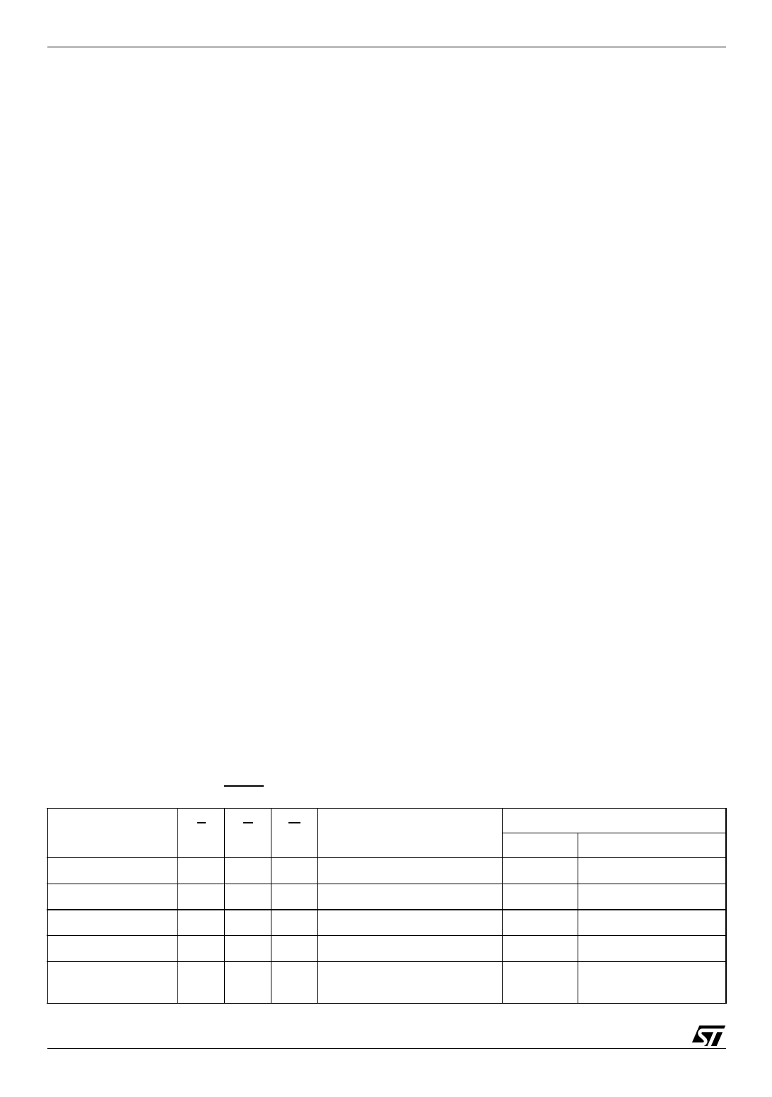
Table 2. Bus Operations, BYTE = VIL
Operation
E
G
W
Address Inputs
DQ15A–1, A0-A21
Bus Read
VIL VIL VIH Cell Address
Bus Write
VIL VIH VIL Command Address
Output Disable
X
VIH
VIH X
Standby
VIH
X
XX
Read Manufacturer
Code
VIL
VIL
VIH
A0 = VIL, A1 = VIL, A9 = VID,
Others VIL or VIH
Data Inputs/Outputs
DQ14-DQ8
DQ7-DQ0
Hi-Z
Data Output
Hi-Z
Data Input
Hi-Z
Hi-Z
Hi-Z
Hi-Z
Hi-Z
20h
10/49
Share Link: