M29W640DT(2004) データシートの表示(PDF) - STMicroelectronics
部品番号
コンポーネント説明
メーカー
M29W640DT
(Rev.:2004)
(Rev.:2004)
STMicroelectronics

M29W640DT Datasheet PDF : 49 Pages
| |||
M29W640DT, M29W640DB
SUMMARY DESCRIPTION
The M29W640D is a 64 Mbit (8Mb x8 or 4Mb x16)
non-volatile memory that can be read, erased and
reprogrammed. These operations can be per-
formed using a single low voltage (2.7 to 3.6V)
supply. On power-up the memory defaults to its
Read mode.
The memory is divided into blocks that can be
erased independently so it is possible to preserve
valid data while old data is erased. Blocks can be
protected in units of 256 KByte (generally groups
of four 64 KByte blocks), to prevent accidental
Program or Erase commands from modifying the
memory. Program and Erase commands are writ-
ten to the Command Interface of the memory. An
on-chip Program/Erase Controller simplifies the
process of programming or erasing the memory by
taking care of all of the special operations that are
required to update the memory contents. The end
of a program or erase operation can be detected
and any error conditions identified. The command
set required to control the memory is consistent
with JEDEC standards.
The device features an asymmetrical blocked ar-
chitecture. The device has an array of 135 blocks:
■ 8 Parameters Blocks of 8 KBytes each (or
4 KWords each)
■ 127 Main Blocks of 64 KBytes each (or
32 KWords each)
M29W640DT has the Parameter Blocks at the top
of the memory address space while the
M29W640DB locates the Parameter Blocks start-
ing from the bottom.
The M29W640D has an extra block, the Extended
Block, (of 32 KWords in x16 mode or of 64 KBytes
in x8 mode) that can be accessed using a dedicat-
ed command. The Extended Block can be protect-
ed and so is useful for storing security information.
However the protection is not reversible, once pro-
tected the protection cannot be undone.
Chip Enable, Output Enable and Write Enable sig-
nals control the bus operation of the memory.
They allow simple connection to most micropro-
cessors, often without additional logic.
The VPP/WP signal is used to enable faster pro-
gramming of the device, enabling double word
programming. If this signal is held at VSS, the boot
block, and its adjacent parameter block, are pro-
tected from program and erase operations.
The memory is delivered with all the bits erased (set
to 1).
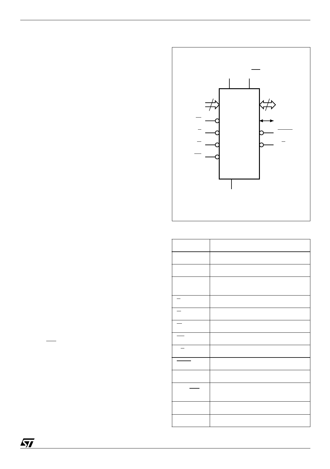
Figure 2. Logic Diagram
VCC VPP/WP
22
A0-A21
15
DQ0-DQ14
W
DQ15A–1
M29W640DT
E
M29W640DB
BYTE
G
RB
RP
VSS
AI05733
Table 1. Signal Names
A0-A21
Address Inputs
DQ0-DQ7 Data Inputs/Outputs
DQ8-DQ14 Data Inputs/Outputs
DQ15A–1
(or DQ15)
Data Input/Output or Address Input
(or Data Input/Output)
E
Chip Enable
G
Output Enable
W
Write Enable
RP
Reset/Block Temporary Unprotect
RB
Ready/Busy Output
BYTE
Byte/Word Organization Select
VCC
Supply Voltage
VPP/WP
Supply Voltage for Fast Program
(optional) or Write Protect
VSS
Ground
NC
Not Connected Internally
5/49
Share Link: