HD74HC589FPEL データシートの表示(PDF) - Renesas Electronics
部品番号
コンポーネント説明
メーカー
HD74HC589FPEL
Renesas Electronics

HD74HC589FPEL Datasheet PDF : 9 Pages
| |||
HD74HC589
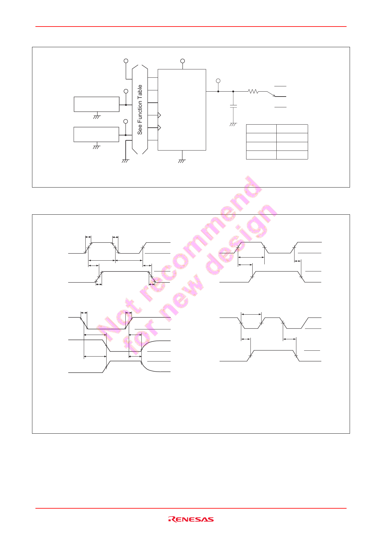
Test Circuit
VCC
Input
Pulse Generator
Zout = 50 Ω
Input
Pulse Generator
Zout = 50 Ω
VCC
OE
Output
SA
QH
Shift/Load
SCK
LCK
A to H
1 k Ω S1
CL =
50 pF
OPEN
GND
VCC
TEST
tPLH / t PHL
tZH/ t HZ
tZL / t LZ
S1
OPEN
GND
VCC
Note : 1. CL includes probe and jig capacitance.
Waveforms
1. (SERIAL SHIFT / PARALLEL LOAD = "L")
Latch
Clock
QH
tr
tf
50% 50%
tW(H)
tPLH
50%
10%
90%
tTLH
50%
tW(L)
tPHL
90% 50%
10%
tTHL
VCC
0V
VOH
VOL
3.
Input G
tf
90%
50%
10%
tZL
tr
10%
90%
50%
tLZ
Waveform - A
Waveform - B
50%
tZH
50%
10%
tHZ
90%
VCC
0V
VOH
VOL
VOH
VOL
2. (SERIAL SHIFT / PARALLEL LOAD = "H")
Shift
Clock
QH
50%
tw
tPLH
50%
50%
50%
tPHL
50%
VCC
0V
VOH
VOL
4.
Serial Shift /
Parallel Load
tw
50%
tPLH
50%
50%
tPHL
Data
50%
50%
VCC
0V
VCC
0V
Notes : 1. Input waveform : PRR ≤ 1 MHz, duty cycle 50%, tr ≤ 6 ns, tf ≤ 6 ns
2. Waveform - A is for an output with internal conditions such that the
output is low except when disabled by the output control.
3. Waveform - B is for an output with internal conditions such that the
output is high except when disabled by the output control.
4. The output are measured one at a time with one transition per measurement.
Rev.2.00 Mar 30, 2006 page 6 of 8
Share Link: