TC7211AM データシートの表示(PDF) - TelCom Semiconductor, Inc
部品番号
コンポーネント説明
メーカー
TC7211AM Datasheet PDF : 7 Pages
| |||
BUS COMPATIBLE, 4-DIGIT
CMOS DECODER/DRIVER
1
TC7211AM
ABSOLUTE MAXIMUM RATINGS*
Supply Voltage ........................................................ +6.5V
Input Voltage, Any Terminal
(Note 2) .................................... V+ +0.3V, GND –0.3V
Power Dissipation TA ≤ 70°C (Note 1) ................... 1.23W
Operating Temperature Range ................ –20°C to +85°C
Storage Temperature Range ................. –65°C to +150°C
Lead Temperature (Soldering, 10 sec) ................. +300°C
*Stresses above those listed under "Absolute Maximum Ratings" may
cause permanent damage to the device. These are stress ratings only, and
functional operation of the device at these or any other conditions above
those indicated in the operational sections of the specifications is not
implied. Exposure to absolute maximum rating conditions for extended
periods may affect device reliability.
NOTES: 1. This limit refers to that of the package and will not be realized
during normal operation.
2. Due to the SCR structure inherent in the CMOS process,
connecting any terminal to voltages greater than V+ or less
than GND may cause destructive latch-up. For this reason, it
is recommended that inputs from external sources not oper-
ating on the same power supply not be applied to the device
before its supply is established, and, in multiple supply
systems, the supply to the TC7211AM be turned on first.
2
3
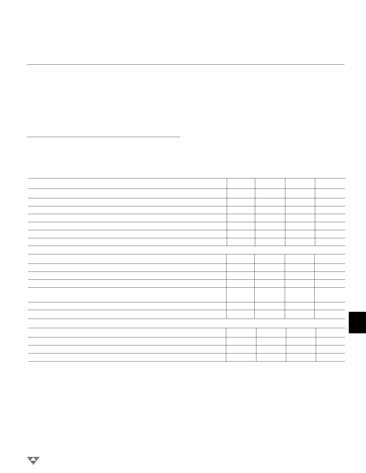
TYPICAL CHARACTERISTICS: All parameters measured with V+ = 5V, TA = 25°C
Symbol
Parameter
Test Conditions
Min
Typ
VSUP
Operating Voltage Range
IOP
Operating Current
IOSCI
Oscillator Input Current
tRFS
Segment Rise/Fall Time
tRFB
Backplane Rise/Fall Time
fOSC
Oscillator Frequency
fBP
Backplane Frequency
Input Characteristics
Display Blank
Pin 36
CL = 200 pF
CL = 5000 pF
Pin 36 Floating
Pin 36 Floating
3
5
—
10
—
±2
—
0.5
—
1.5
—
16
—
125
VIH
Logic “1” High Input Voltage
VIL
Logic “0” Low Input Voltage
IILK
Input Leakage Current
Pins 27–34
3
—
—
—
—
±0.01
CIN
IBPLK
Input Capacitance
BP Input Current
Leakage
Pins 27–34
Measured at Pin 5 With
Pin 36 at GND
—
5
—
±0.01
CBPI
BP Input Capacitance
All Devices
—
200
AC Characteristics
Symbol
Parameter
Test Conditions
tCSA
Chip Select Active Pulse Width (Note 1)
tDS
Data Setup Time
tDH
Data Hold Time
tICS
Inter-Chip Select Time
NOTE: 1. Other chip select (CS) is either held at logic zero or both CS1 and CS2 driven together.
200
—
100
—
10
0
2
—
Max
Unit
6
V
50
±10
µA
µA
4
—
µsec
—
µsec
—
kHz
—
Hz
—
1
V
V
5
±1
µA
—
pF
±1
µA
—
pF
6
—
nsec
—
nsec
—
nsec
—
µsec
7
TELCOM SEMICONDUCTOR, INC.
8
6-9
Share Link: 