CXD3172AR データシートの表示(PDF) - Sony Semiconductor
部品番号
コンポーネント説明
メーカー
CXD3172AR Datasheet PDF : 25 Pages
| |||
CXD3172AR
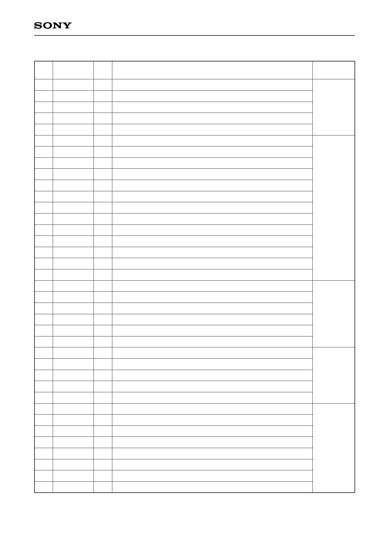
Pin Description
Pin
No.
Symbol
1 VRT
2 AVD1
3 VIN
4 AVS1
5 VRB
6 CSROM
7 CASI
8 CASO
9 CASCK
10 VSS1
11 XRST
12 TEST1
13 SIFSEL
14 VDD1
15 XCS
16 SI
17 SO
18 SCK
19 RG
20 REFC
21 AVD2
22 H1
23 H2
24 AVS2
25 XRS
26 AVS3
27 XSHD
28 XSHP
29 AVD3
30 VM
31 V4
32 V2
33 V3
34 VH
35 V1
36 SUB
37 VL
I/O
Description
Power supply
I A/D converter reference voltage (top) input.
— Power supply for A/D converter.
I Analog signal input. (for A/D converter)
— GND
I A/D converter reference voltage (bottom) input.
O Chip select output for camera peripheral ICs. (to EEPROM)
I Serial data input for system communication.
O Serial data output for system communication.
O Serial clock output for system communication.
— GND
I Reset input.
I Test
I Serial interface mode switching. 0: microcomputer (3 wires) 1: RS232C
— Power supply for logic.
I Chip select input for 3 wires serial interface. (when SIFSEL = 0)
I Serial data input for 3 wires serial interface. (when SIFSEL = 0)
O Serial data output for 3 wires serial interface. (when SIFSEL = 0)
I/O Serial clock input for 3 wires serial interface. (when SIFSEL = 0)
O Reset gate pulse output.
I Capacitor connection.
— Power supply for horizontal driving pulse. (3.3V/5.0V)
O CCD horizontal register transfer pulse output.
O CCD horizontal register transfer pulse output.
— GND
O Resampling pulse output.
— GND
O Data sample-and-hold pulse output.
O Precharge level sample-and-hold pulse output.
— Power supply for sample-and-hold pulse.
— V-Driver Middle level power supply.
O CCD vertical register transfer pulse output.
O CCD vertical register transfer pulse output.
O CCD vertical register transfer pulse output.
— V-Driver High level power supply.
O CCD vertical register transfer pulse output.
O CCD electronic shutter pulse output.
— V-Driver Low level power supply.
–4–
AVD1
AVS1
VDD1
VSS1
AVD2
AVS2
AVD3
AVS3
VH
VL
VM
Share Link: 