MAX2027 データシートの表示(PDF) - Maxim Integrated
部品番号
コンポーネント説明
メーカー
MAX2027 Datasheet PDF : 10 Pages
| |||
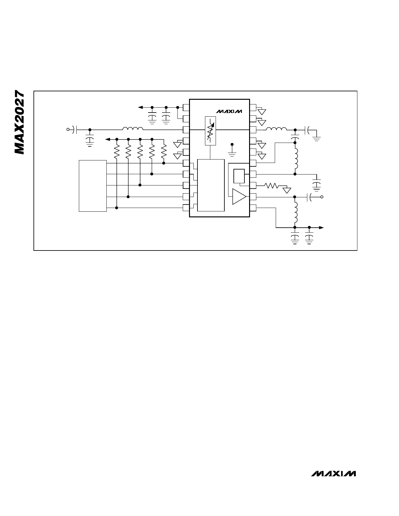
IF Digitally Controlled Variable-Gain Amplifier
C1
RF IN
C8*
VCC
CONTROL
INPUTS
VCC
C7
L3*
1
C2
2
3
4
R6 R5 R4 R3 R2
5
6
B4
B3 7
B2 8
9
B1
B0 10
20
MAX2027
19
L4*
C9*
EXPOSED
PADDLE
18 ATTNOUT
17
C3
ATTENUATION
LOGIC
CONTROL
16
15 AMPIN
AMP
BIAS
14 IBIAS
13
ISET R1
12
11
L1
C4
L2
C10
RF OUT
*OPTIONAL COMPONENTS: USE TO IMPROVE HIGHER FREQUENCY MATCHING
VCC
C5
C6
Figure 1. Typical Application Circuit
Fixed-Gain Amplifier
The MAX2027 integrates a fixed-gain amplifier in a neg-
ative feedback topology. This fixed-gain amplifier is
optimized for a frequency range of operation from
50MHz to 400MHz with a high-output third-order inter-
cept point (OIP3). The bias current is chosen to opti-
mize the IP3 of the amplifier. When R1 is 825Ω, the
current consumption is 60mA while exhibiting a typical
35dBm output IP3.
Choke Inductor
The fixed-gain amplifier output port requires an external
pullup choke inductor to VCC. At the input, connect a
bias inductor of 330nH from AMPIN (pin 15) to IBIAS
(pin 14). At the output, connect a 680nH choke inductor
from RF_OUT (pin 12) to VCC (pin 11) to provide bias
current to the amplifier.
Layout Considerations
A properly designed PC board is an essential part of
any RF/microwave circuit. Keep RF signal lines as short
as possible to reduce losses, radiation, and induc-
tance. For the best performance, route the ground pin
traces directly to the exposed pad under the package.
The PC board exposed pad must be connected to the
ground plane of the PC board. It is suggested that multi-
ple vias be used to connect this pad to the lower level
ground planes. This method provides a good RF/thermal
conduction path for the device. Solder the exposed pad
on the bottom of the device package to the PC board.
The MAX2027 Evaluation Kit can be used as a refer-
ence for board layout. Gerber files are available upon
request at www.maxim-ic.com.
Power-Supply Bypassing
Proper voltage-supply bypassing is essential for high-
frequency circuit stability. Bypass each VCC pin with a
0.1µF and 100pF capacitor. Connect the 100pF capacitor
as close to VCC pins as possible.
Exposed Pad RF/Thermal Considerations
The exposed paddle (EP) of the MAX2027’s 20-pin
TSSOP-EP package provides a low thermal-resistance
path to the die. It is important that the PC board on
8 _______________________________________________________________________________________
Share Link: 