MAX6886 データシートの表示(PDF) - Maxim Integrated
部品番号
コンポーネント説明
メーカー
MAX6886 Datasheet PDF : 13 Pages
| |||
Pin-Selectable, Hex Power-Supply
Supervisory Circuit
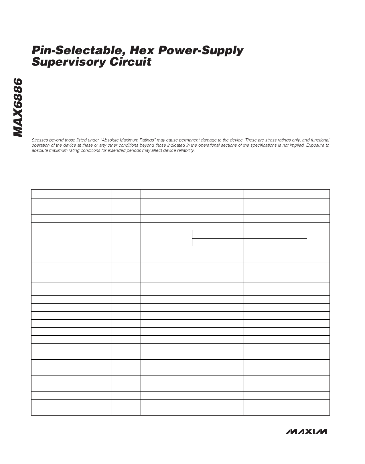
ABSOLUTE MAXIMUM RATINGS
(All voltages referenced to GND.)
IN1–IN6, VCC, RESET, SRT, SWT .............................-0.3V to +6V
TH0–TH4, WDI, MR, MARGIN ..................................-0.3V to +6V
DBP ..........................................................................-0.3V to +3V
Input/Output Current (all pins)..........................................±20mA
Continuous Power Dissipation (TA = +70°C)
20-Pin 5mm x 5mm Thin QFN
(derate 21.3mW/°C above +70°C) .............................1702mW
Maximum Junction Temperature .....................................+150°C
Operating Temperature Range ...........................-40°C to +85°C
Storage Temperature Range .............................-65°C to +150°C
Lead Temperature (soldering, 10s) .................................+300°C
Stresses beyond those listed under “Absolute Maximum Ratings” may cause permanent damage to the device. These are stress ratings only, and functional
operation of the device at these or any other conditions beyond those indicated in the operational sections of the specifications is not implied. Exposure to
absolute maximum rating conditions for extended periods may affect device reliability.
ELECTRICAL CHARACTERISTICS
(VIN1–VIN4 or VCC = 2.7V to 5.8V, WDI = GND, TH0–TH4 = MARGIN = MR = DBP, TA = -40°C to +85°C, unless otherwise noted.
Typical values are at TA = +25°C.) (Notes 1, 2)
PARAMETER
Operating Voltage Range
(Note 3)
Supply Current
Digital Bypass Voltage
Threshold Accuracy (Table 2)
Threshold Hysteresis
Threshold Tempco
IN_ Input Impedance
IN_ Input Leakage Current
Power-Up Delay
IN_ to RESET Delay
Reset Default Timeout Period
Reset Adjustable Timeout Period
SRT Adjustable Timeout Current
SRT Default Timeout Threshold
SRT Adjustable Timeout
Threshold
SYMBOL
ICC
VDBP
VTH
VTH-HYS
∆VTH/°C
RIN
IIN
tD-PO
tD-R
tRP
tRP-ADJ
ISRT
VSRT-DEF
CONDITIONS
Voltage on either one of IN1–IN4 or VCC to
guarantee the part is fully operational
VIN1 = 5.8V, IN2–IN6 = GND, no load
IN1–IN6, VIN _ falling
TA = +25oC to +85oC
TA = -40oC to +85oC
For VIN_ < highest VIN1–IN4 and VIN_ < VCC
(not ADJ), thresholds are not set as
adjustable
IN5, IN6
IN1–IN4 set as adjustable thresholds
VCC ≥ 2.5V
IN_ falling/rising, 100mV overdrive
VSRT = VCC
CSRT = 47nF
VSRT = VGND
VSRT ≥ VSRT-DEF, selects reset default
VSRT-ADJ (Note 4)
MIN
2.7
2.48
-1
-1.5
130
-150
180
135
180
1.1
0.95
TYP MAX UNITS
5.8
V
0.9
2.55
0.3
10
1.2
2.67
+1
+1.5
mA
V
% VTH
% VTH
ppm/°C
200 300
kΩ
+150
nA
2.5
ms
20
µs
200 220
ms
207 280
ms
230 280
nA
1.25 1.5
V
1.00 1.05
V
SRT Adjustable Timeout
Discharge Threshold
VSRT-DIS (Note 5)
100
mV
SRT Adjustable Timeout Output-
Low Discharge Current
RESET Output Low
RESET Output Open-Drain
Leakage Current
ISRT-DIS VSRT = 0.3V
VOLRESET ISINK = 4mA, output asserted
ILKG Output tri-stated
0.7
mA
0.4
V
-1
+1
µA
2 _______________________________________________________________________________________
Share Link: 