MAX2121 データシートの表示(PDF) - Maxim Integrated
部品番号
コンポーネント説明
メーカー
MAX2121 Datasheet PDF : 18 Pages
| |||
Complete Direct-Conversion L-Band Tuner
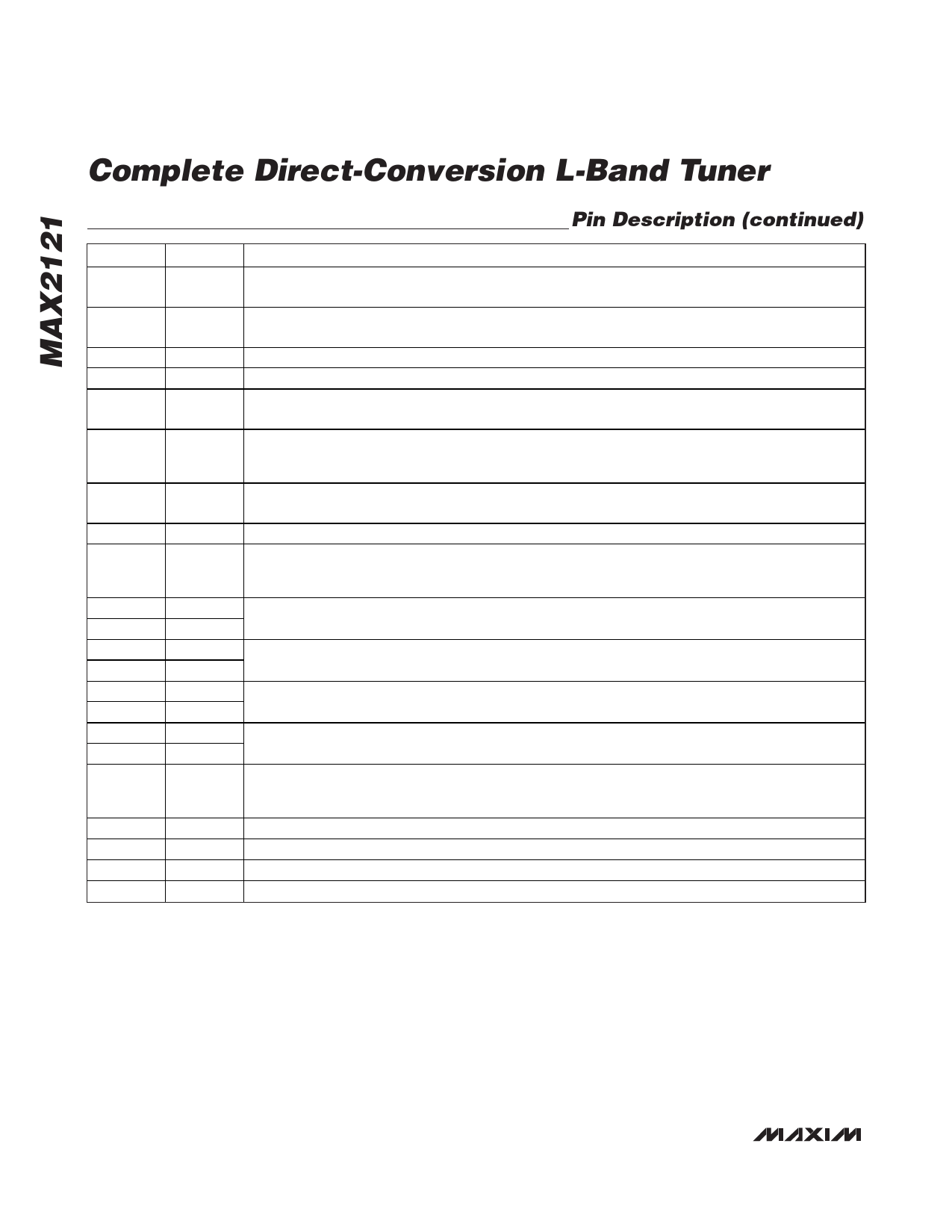
Pin Description (continued)
PIN
NAME
FUNCTION
8
BYPVCO
Internal VCO Bias Bypass. Bypass to GND with a 100nF capacitor connected as close as possible to
the pin. Do not share capacitor ground vias with other ground connections.
9
TUNEVCO
High-Impedance VCO Tune Input. Connect the PLL loop filter output directly to this pin with as short of
a connection as possible.
10
GNDTUNE Ground for TUNEVCO. Connect to the PCB ground plane.
11
GNDSYN Ground for Synthesizer. Connect to the PCB ground plane.
12
CPOUT
Charge-Pump Output. Connect this output to the PLL loop filter input with the shortest
connection possible.
DC Power Supply for Synthesizer Circuits. Connect to a +3.3V low-noise supply. Bypass to GND with
13
VCC_SYN a 1nF capacitor connected as close as possible to the pin. Do not share capacitor ground vias with
other ground connections.
14
XTAL
Crystal-Oscillator Interface. Use with an external parallel-resonance-mode crystal through a series
1nF capacitor. See the Typical Application Circuit.
15
REFOUT Crystal-Oscillator Buffer Output. A DC-blocking capacitor must be used when driving external circuitry.
DC Power Supply for Digital Logic Circuits. Connect to a +3.3V low-noise supply. Bypass to GND with
16
VCC_DIG a 1nF capacitor connected as close as possible to the pin. Do not share capacitor ground vias with
other ground connections.
17
QOUT+
Quadrature Baseband Differential Output. AC-couple with 47nF capacitors to the demodulator input.
18
QOUT-
19
IOUT+
In-Phase Baseband Differential Output. AC-couple with 47nF capacitors to the demodulator input.
20
IOUT-
21
IDC+
I-Channel Baseband DC Offset Correction. Connect a 47nF ceramic chip capacitor from IDC- to IDC+.
22
IDC-
23
QDC+
Q-Channel Baseband DC Offset Correction. Connect a 47nF ceramic chip capacitor from QDC- to QDC+.
24
QDC-
DC Power Supply for Baseband Circuits. Connect to a +3.3V low-noise supply. Bypass to GND with
25
VCC_BB a 1nF capacitor connected as close as possible to the pin. Do not share capacitor ground vias with
other ground connections.
26
SDA 2-Wire Serial-Data Interface. Requires 1k pullup resistor to VCC.
27
SCL 2-Wire Serial-Clock Interface. Requires 1k pullup resistor to VCC.
28
ADDR Address. Must be connected to either ground (logic 0) or supply (logic 1).
—
EP
Exposed Pad. Solder evenly to the board’s ground plane for proper operation.
8 _______________________________________________________________________________________
Share Link: 