LR645 データシートの表示(PDF) - Supertex Inc
部品番号
コンポーネント説明
メーカー
LR645 Datasheet PDF : 9 Pages
| |||
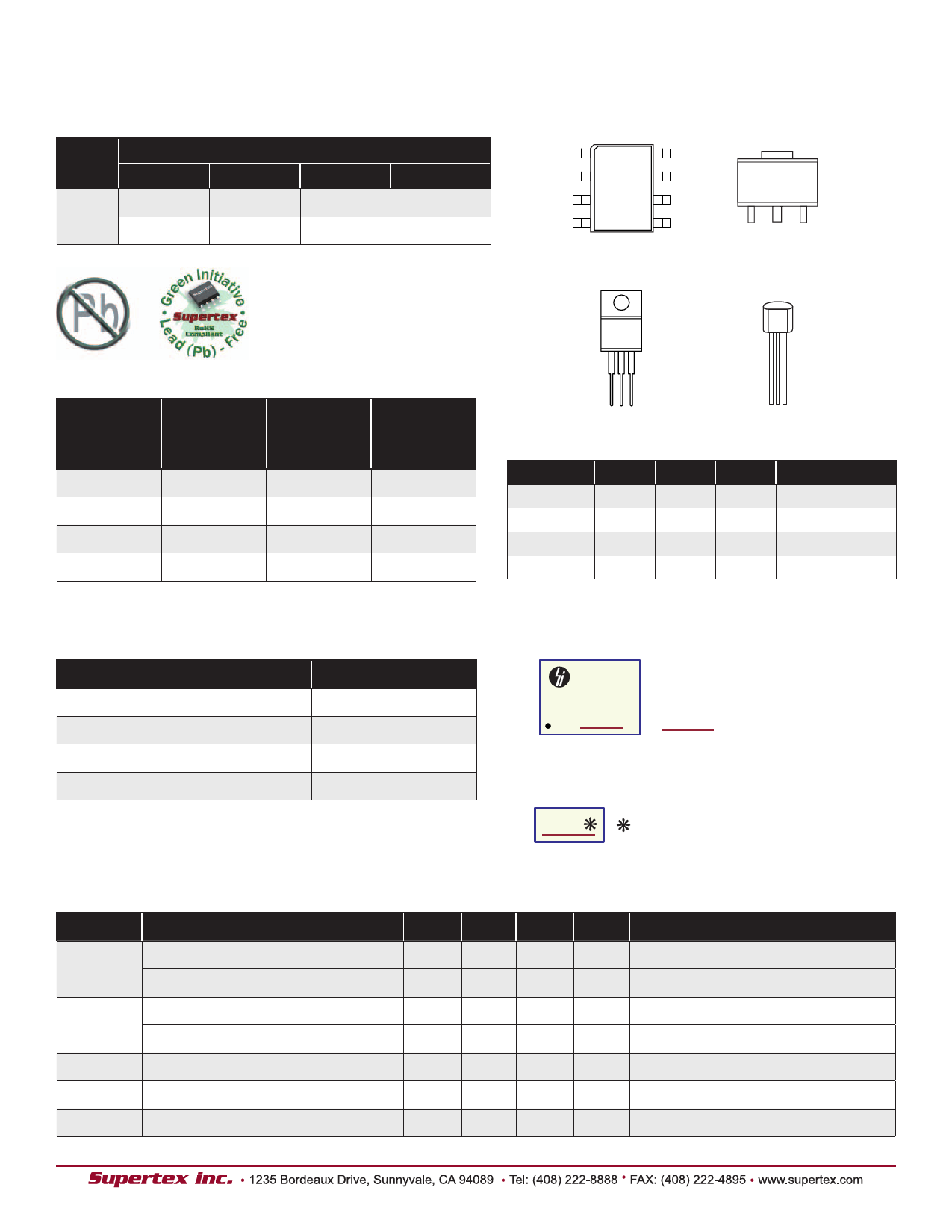
Ordering Information
Device
TO-92
Package Option
TO-243AA TO-220 8-Lead SOIC
LR645N3 LR645N8 LR645N5 LR645LG
LR645
LR645N3-G LR645N8-G LR645N5-G LR645LG-G
-G indicates package is RoHS compliant (‘Green’)
Pin Configurations
1
8
8-Lead SOIC
TAB
LR645
TAB
12 3
TO-243AA
(SOT-89)
Thermal Characteristics
Package
SOIC
Power
Dissipation
@TA = 25OC
0.31W
θJC
OC/W
156
TO-92
0.74W
125
TO-220
1.8W
8.3
TO-243AA
1.6W
15
* Mounted on FR4 board; 25mm x 25mm x 1.57mm
Significant PD increase possible on ceramic substrate
θJA
OC/W
400*
170
70
78*
Absolute Maximum Ratings
Parameter
Value
Input voltage
450V
Output voltage
15.5V
Operating and storage temperature
-55°C to +150OC
13
2
TO-220
13
2
TO-92
TO-92
+VIN
1
GND
2
VOUT
3
TO-243AA 1 2, TAB 3
TO-220
1 2, TAB 3
8-Lead SO 1
3
4
TRIM
-
-
-
5
GATE
-
-
-
7
Package Markings
YYWW
LR645
LLLL
YY = Year Sealed
WW = Week Sealed
L = Lot Number
= “Green” Packaging
8-Lead SOIC
Soldering temperature
300OC
Absolute Maximum Ratings are those values beyond which damage to the device may
occur. Functional operation under these conditions is not implied. Continuous operation
of the device at the absolute rating level may affect device reliability. All voltages are
referenced to device ground.
LR6
Electrical Characteristics
(Test conditions unless otherwise specified: T = 25°C; V = 15 to 450V, C = 0.01µF)
A
IN
OUT
Symbol Parameter
Min Typ Max
Units
= 2-week alpha date code
TO-243AA
Conditions
VOUT
ΔVOUT
VIN
IINQ
IOFF
Output voltage
Output voltage over temperature1
Line regulation
Load regulation
Operating input voltage range
Input quiescent current
VIN off-state leakage current
9.3 10 10.7 V No load
9.0 10 11.5 V TJ = - 40°C ≤ to + 125°C, No load
-
40 200 mV VIN = 15V to 400V, No load
-
150 400 mV VIN = 50V, IOUT = 0 to 3.0mA
15
-
450
V ---
-
50 150 µA No Load
-
0.1
10
µA VAUX ≥ VOUT +1V applied to VOUT pin
2
Share Link: 