LR645 データシートの表示(PDF) - Supertex Inc
部品番号
コンポーネント説明
メーカー
LR645 Datasheet PDF : 9 Pages
| |||
LR645
Symbol Parameter
Min Typ Max
IAUX
Input current to VOUT
-
-
200
ΔVOUT/
ΔVIN
Ripple rejection ratio1
50 60
-
en
Noise voltage1
-
25
-
IPEAK
Output peak current2
-
30
-
VAUX
External voltage applied to VOUT
-
- 13.2
8-lead, adjustable output voltage version only:
Test conditions unless otherwise specified: TA = 25°C; VIN = 15 to 450V, COUT = 0.01µF
VOUT
Output regulation trim range1
8
-
12
ΔV
OUT
Load regulation at 8V trim1
Load regulation at 12V trim1
-
200 400
-
100 400
Notes:
1. Guaranteed by design, not tested in production.
2. Pulse test duration < 1.0msec, Duty cycle < 2%
Units Conditions
µA VAUX ≥ VOUT +1V applied to VOUT pin
dB 120Hz, No Load
µV 0.01 to 100KHz
mA COUT = 10µF, VIN = 400V
V ---
V No load
mV VIN = 15V, IOUT = 0 to 1.0mA
mV VIN = 50V, IOUT = 0 to 3.0mA
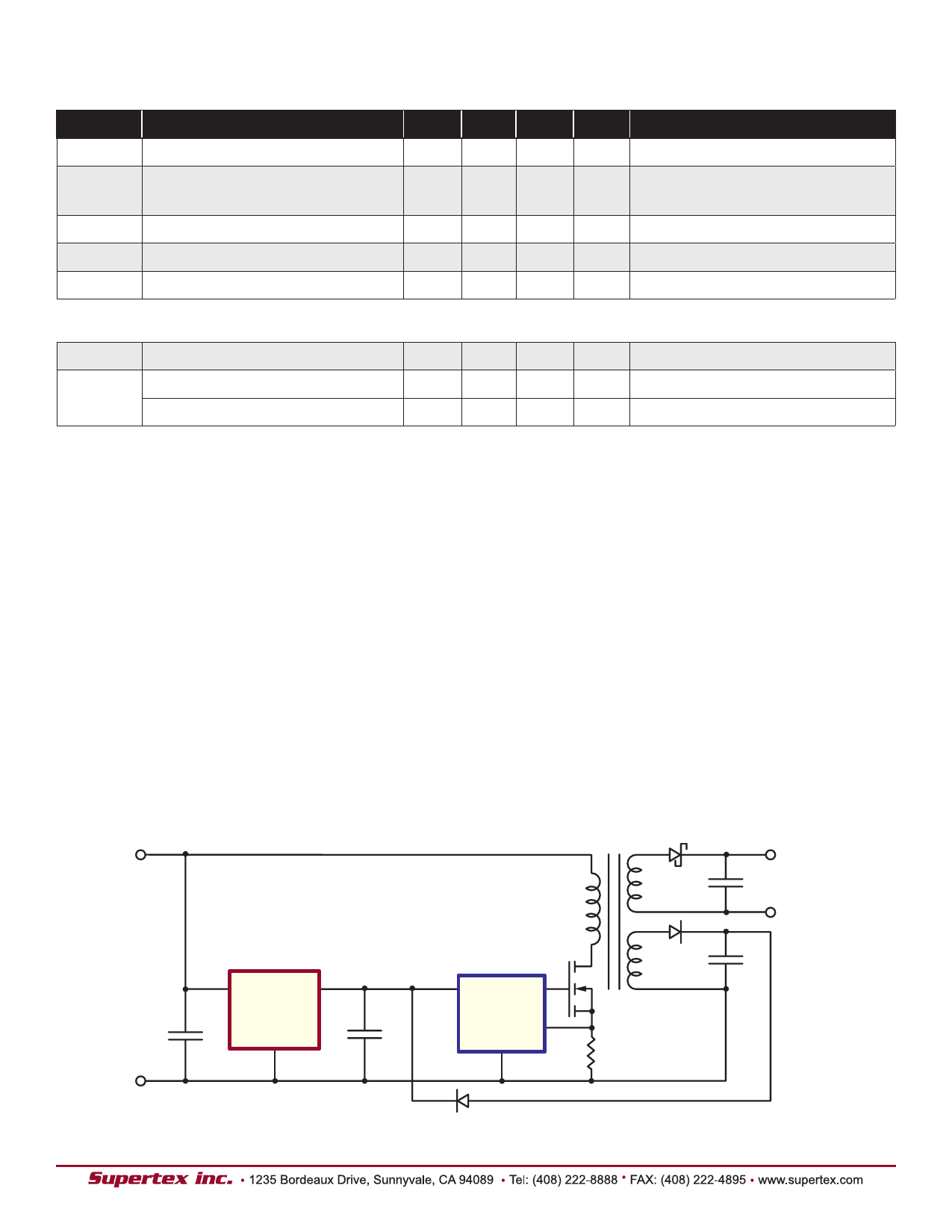
LR645: SMPS Start-Up Circuit
One of the main applications for the LR645 is a start-up
circuit for off-line switch-mode power supplies (SMPS), as
shown in Figure1. A minimum output capacitance of 0.01µF
is recommended for stability. The wide operating input volt-
age range of the LR645 allows the SMPS to operate and
start-up from rectified AC or a DC voltage of 15V to 450V
without adjustment.
During start-up, the LR645 powers the VCC line of the PWM
IC with a nominal output voltage of 10V. The auxiliary voltage
connected through a diode to the VOUT pin of the LR645 will
start to increase. When the auxiliary voltage becomes larger
than the output voltage the LR645 turns OFF its internal high
voltage input line and output voltage, allowing the auxiliary
voltage to power the VCC line of the PWM IC. The input cur-
rent drawn by the LR645 from the high voltage line after
start-up will therefore only be leakage current of the internal
MOSFET switch, which is typically 0.1µA.
The 3-terminal version shown in Figure 1 has load regula-
tion guaranteed from 0 to 3.0mA at a fixed nominal output
voltage of 10V. Applications requiring higher output current
and/or a different output voltage can use the 8 pin adjustable
version.
Figure 1: SMPS Start-Up Circuit
+
15V
to
VIN
450V
CIN
–
LR6
GND
VCC
PWM IC
COUT
+
5.0V
–
VAUX = 12V
3
Share Link: 