AD537SD/883B データシートの表示(PDF) - Analog Devices
部品番号
コンポーネント説明
メーカー
AD537SD/883B Datasheet PDF : 8 Pages
| |||
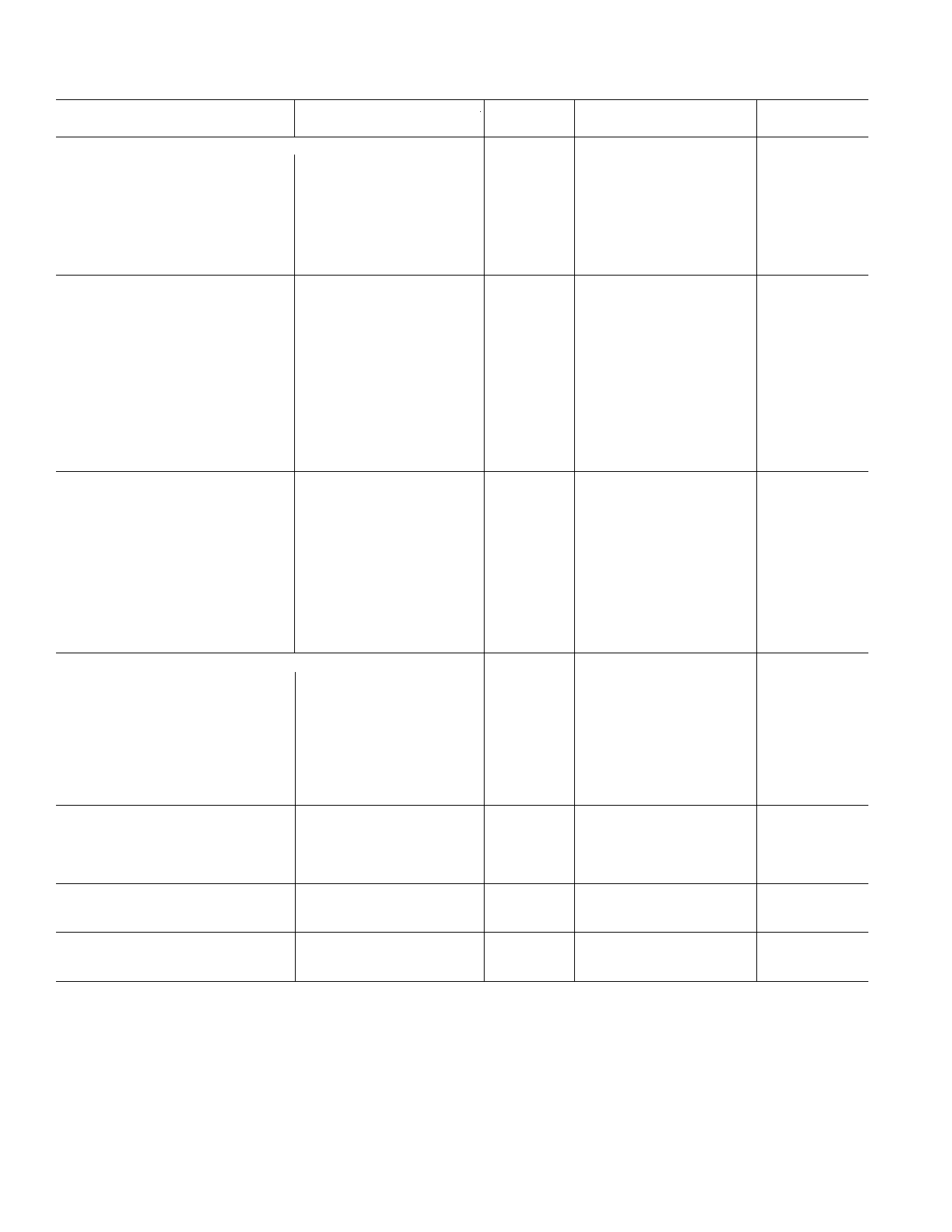
AD537–SPECIFICATIONS (typical @ +25؇C with VS (total) = 5 V to 36 V, unless otherwise noted)
Model
AD537JH
AD537JD
AD537KD
AD537KH
CURRENT-TO-FREQUENCY CONVERTER
Frequency Range
Nonlinearity1
0 kHz to 150 kHz
fMAX = 10 kHz
fMAX = 100 kHz
Full-Scale Calibration Error
C = 0.01 µF, IIN = 1.000 mA
vs. Supply (fMAX < 100 kHz)
vs. Temp (TMIN to TMAX)
0.15% max (0.1% typ)
0.25% max (0.15% typ)
± 10% max
± 0.1%/V max (0.01% typ)
± 150 ppm/°C max (50 ppm typ)
ANALOG INPUT AMPLIFIER
(Voltage-to-Current Converter)
Voltage Input Range
Single Supply
Dual Supply
Input Bias Current
0 to (+VS – 4) Volts (min)
–VS to (+VS – 4) Volts (min)
(Either Input)
Input Resistance (Noninverting)
100 nA
250 MΩ
Input Offset Voltage
(Trimmable in “D” Package Only)
vs. Supply
vs. Temp (TMIN to TMAX)
Safe Input Voltage3
5 mV max
200 µV/V max
5 µV/°C
± VS
REFERENCE OUTPUTS
Voltage Reference
Absolute Value
vs. Temp (TMIN to TMAX)
vs. Supply
Output Resistance4
Absolute Temperature Reference5
1.00 Volt ± 5% max
50 ppm/°C
± 0.03%/V max
380 Ω
Nominal Output Level
1.00 mV/K
Initial Calibration @ +25°C
Slope Error from 1.00 mV/K
Slope Nonlinearity
Output Resistance5
298 mV (± 5 mV)
± 0.02 mV/K
± 0.1 K
900 Ω
*
*
*
± 7% max
*
*
*
*
*
*
*
100 µV/V max
*
*
*
*
*
*
*
*
*
*
*
*
0.07% max
0.1% max
± 5% max
*
50 ppm/°C max (30 ppm typ)2
*
*
*
*
2 mV max
100 µV/V max
1 µV/°C
*
*
100 ppm/°C max
*
*
*
298 mV (± 5 mV max)
*
*
*
OUTPUT INTERFACE (Open Collector Output)
(Symmetrical Square Wave)
Output Sink Current in Logic “0”
VOUT = 0.4 V max (TMIN to TMAX) 20 mA min
Output Leakage Current in Logic “1”
(TMIN to TMAX)
Logic Common Level Range
Rise/Fall Times (CT = 0.01 µF)
IIN = l mA
IIN = 1 µA
200 nA max
–VS to (+VS – 4) Volts
0.2 µs
1 µs
POWER SUPPLY
Voltage, Rated Performance
Single Supply
4.5 V to 36 V
Dual Supply
± 5 V to ± 18 V
Quiescent Current
1.2 mA (2.5 mA max)
20 mA min
*
*
*
*
20 mA min
*
*
*
*
*
*
*
*
*
*
TEMPERATURE RANGE
Rated Performance
Storage
PACKAGE OPTIONS6, 7
TO-116 Ceramic DIP (D-14)
TO-100 Header (H-10A)
0°C to +70°C
–65°C to +150°C
AD537JH
*
*
AD537JD
*
*
AD537KD
AD537KH
AD537SD1
AD537SH1
*
**
**
**
*
250 ppm/°C max
*
*
*
*
**
**
10 µV/°C max
*
*
**
*
*
*
**
*
*
*
10 mA min
2 µA max
*
*
*
*
*
*
–55°C to +125°C
*
AD537SD
AD537SH
NOTES
*Specifications same as AD537JH.
**Specifications same as AD537K.
1Nonlinearity is specified for a current input level (IIN) to the converter from 0.1 µA to 1000 µA. Converter has 100% overrange capability up to IIN = 2000 µA with slightly
reduced linearity. Nonlinearity is defined as deviation from a straight line from zero to full scale, expressed as a percentage of full scale.
2Guaranteed not tested.
3Maximum voltage input level is equal to the supply on either input terminal. However, large negative voltage levels can be applied to the negative terminal if the input is scaled to
a nominal 1 mA full scale through an appropriate value resistor (See Figure 2).
4Loading the 1.0 volt or 1 mV/K outputs can cause a significant change in overall circuit performance, as indicated in the applications section. To maintain normal operation,
these outputs should be operated into the external buffer or an external amplifier.
5Temperature reference output performance is specified from 0°C to +70°C for “J” and “K” devices, –55°C to +125°C for “S” model.
6D = Ceramic DIP; H = Hermetic Metal Can. For outline information see Package Information section.
7For AD537/883B specifications, refer to Analog Devices Military Products Databook.
Specifications subject to change without notice.
–2–
REV. 0
Share Link: 