MXSMBJSAC26E3 データシートの表示(PDF) - Microsemi Corporation
部品番号
コンポーネント説明
メーカー
MXSMBJSAC26E3 Datasheet PDF : 7 Pages
| |||
MSMBJSAC5.0 – MSMBJSAC75(e3)
Symbol
CT
I (BR)
ID
I PP
P PP
V (BR)
VC
VWM
SYMBOLS & DEFINITIONS
Definition
Total Capacitance: The total small signal capacitance between the diode terminals of a complete device.
Breakdown Current: The current used for measuring Breakdown Voltage V(BR).
Standby Current: The current through the device at rated stand-off voltage.
Peak Impulse Current: The maximum rated random recurring peak impulse current or nonrepetitive peak impulse
current that may be applied to a device. A random recurring or nonrepetitive transient current is usually due to an
external cause, and it is assumed that its effect will have completely disappeared before the next transient arrives.
Peak Pulse Power. The rated random recurring peak impulse power or rated nonrepetitive peak impulse power. The
impulse power is the maximum-rated value of the product of IPP and VC.
Breakdown Voltage: The voltage across the device at a specified current I(BR) in the breakdown region.
Clamping Voltage: The voltage across the device in a region of low differential resistance during the application of an
impulse current (IPP) for a specified waveform.
Working Standoff Voltage: The maximum-rated value of dc or repetitive peak positive cathode-to-anode voltage that
may be continuously applied over the standard operating temperature.
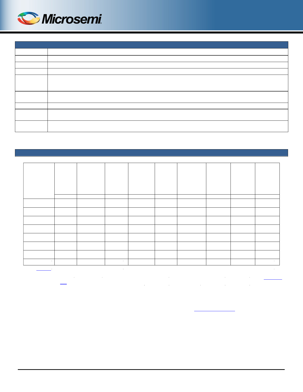
ELECTRICAL CHARACTERISTICS @ 25 oC unless otherwise stated
PART
NUMBER
WORKING
STAND-
OFF
VOLTAGE
(Note 1)
V WM
BREAKDOWN
VOLTAGE
V BR @ I BR
1.0mA
V (BR)
MAXIMUM
STANDBY
CURRENT
I D @ V WM
MAXIMUM
CLAMPING
VOLTAGE
VC @ IP = 5.0A
MAXIMUM
PEAK
PULSE
CURRENT*
RATING
(Note 2)
I PP
MAXIMUM
CAPACITANCE
@ 0 Volts
f = 1 MHz
CT
WORKING
INVERSE
BLOCKING
VOLTAGE
V WIB
INVERSE
BLOCKING
LEAKAGE
CURRENT
@ V WIB
I IB
PEAK
INVERSE
BLOCKING
VOLTAGE
V PIB
Volts
Volts (min)
µA
Volts
Amps
pF
MSMBJSAC5.0
5.0
7.60
300
10.0
44
30
MSMBJSAC6.0
6.0
7.90
300
11.2
41
30
MSMBJSAC7.0
7.0
8.33
300
12.6
38
30
MSMBJSAC8.0
8.0
8.89
100
13.4
36
30
MSMBJSAC8.5
8.5
9.44
50
14.0
34
30
MSMBJSAC10
10
11.10
5.0
16.3
29
30
MSMBJSAC12
12
13.30
5.0
19.0
25
30
MSMBJSAC15
15
16.70
5.0
23.6
20
30
MSMBJSAC18
18
20.00
5.0
28.8
15
30
MSMBJSAC22
22
24.40
5.0
35.4
14
30
MSMBJSAC26
26
28.90
5.0
42.3
11.1
30
MSMBJSAC36
36
40.0
5.0
60.0
8.6
30
MSMBJSAC45
45
50.00
5.0
77.0
6.8
30
MSMBJSAC50
50
55.50
5.0
88.0
5.8
30
MSMBJSAC75
75
83.3
5.0
121
4.1
30
Volts
µA
Volts
75
10
100
75
10
100
75
10
100
75
10
100
75
10
100
75
10
100
75
10
100
75
10
100
75
10
100
75
10
100
75
10
100
75
10
100
150
10
200
150
10
200
150
10
200
*See Figure 3. For the MSMBJSAC75, the maximum clamping voltage VC is at the maximum rated Peak Pulse Current (IPP) of 4.1 Amps.
Clamping Factor: The ratio of the numerical value of VC to V(BR) is typically 1.4 @ full rated power, 1.20 @ 50% rated power. Also see MicroNote
108.
Note 1: A Transient Voltage Suppressor is normally selected according to voltage (VWM), which should be equal to or greater than the dc or
continuous peak operating voltage level.
Note 2: Test in TVS avalanche direction. Do not pulse in “forward” direction. See section for Application Schematics herein.
RF01021, Rev. B (8/15/13)
©2013 Microsemi Corporation
Page 3 of 7
Share Link: 