1.5SMC82A-CT7 データシートの表示(PDF) - Unspecified
部品番号
コンポーネント説明
メーカー
1.5SMC82A-CT7 Datasheet PDF : 6 Pages
| |||
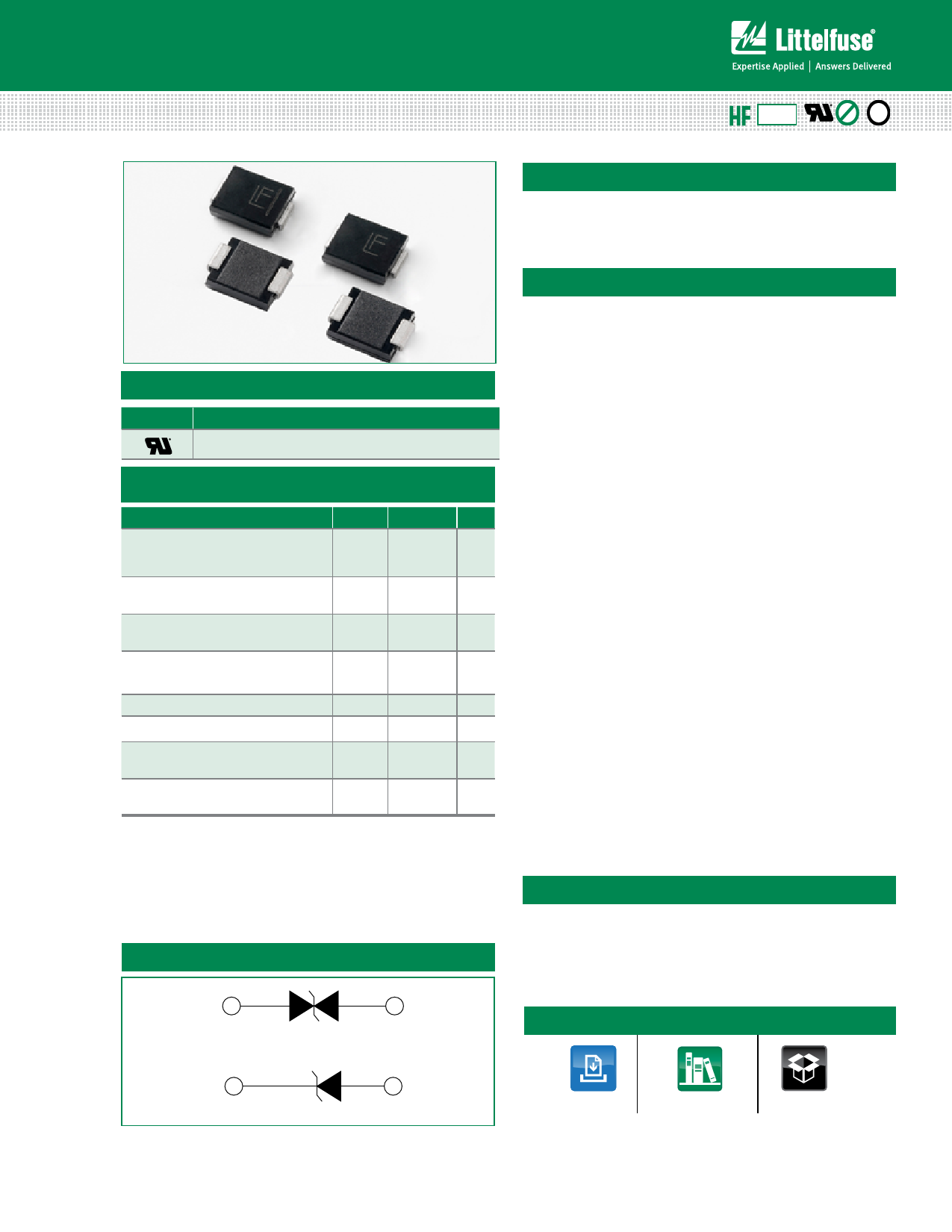
Transient Voltage Suppression Diodes
Surface Mount – 1500W > 1.5SMC series
1.5SMC Series
RoHS
Pb e3
Uni-directional
Bi-directional
Agency Approvals
AGENCY
AGENCY FILE NUMBER
E230531
Maximum Ratings and Thermal Characteristics
(TA=25OC unless otherwise noted)
Parameter
Symbol Value Unit
Peak Pulse Power Dissipation at
TA=25ºC by 10/1000µs Waveform
PPPM
1500
W
(Fig.2)(Note 1), (Note 2), (Note 5)
Power Dissipation on Infinite Heat
Sink at TL=50OC
PD
Peak Forward Surge Current, 8.3ms
Single Half Sine Wave (Note 3)
IFSM
Maximum Instantaneous Forward
Voltage at 100A for Unidirectional
VF
Only (Note 4)
Operating Temperature Range
TJ
Storage Temperature Range
TSTG
6.5
W
200
A
3.5/5.0 V
-65 to 150 °C
-65 to 175 °C
Typical Thermal Resistance Junction
to Lead
RθJL
15
°C/W
Typical Thermal Resistance Junction
to Ambient
RθJA
75
°C/W
Notes:
1. Non-repetitive current pulse , per Fig. 4 and derated above TJ (initial) =25OC per Fig. 3.
2. Mounted on copper pad area of 0.31x0.31” (8.0 x 8.0mm) to each terminal.
3. Measured on 8.3ms single half sine wave or equivalent square wave for unidirectional
device only, duty cycle=4 per minute maximum.
4. VF < 3.5V for single die parts and VF< 5.0V for stacked-die parts.
5. The PPPM of stacked-die parts is 2000W and please contact littelfuse for the detail
stacked-die parts.
Functional Diagram
Cathode
Bi-directional
Uni-directional
Anode
Descriptios
The 1.5SMC series is designed specifically to protect
sensitive electronic equipment from voltage transients
induced by lightning and other transient voltage events.
Features
• 1500W peak pulse power
capability at 10/1000μs
waveform, repetition rate
(duty cycles):0.01%
• Excellent clamping
capability
• Low incremental surge
resistance
• Typical IR less than 1μA
when VBR min>12V
• For surface mounted
applications to optimize
board space
• Low profile package
• Built-in strain relief
• Typical failure mode is
short from over-specified
voltage or current
• Whisker test is conducted
based on JEDEC
JESD201A per its table 4a
and 4c
• IEC-61000-4-2 ESD
30kV(Air), 30kV (Contact)
• ESD protection of data
lines in accordance with
IEC 61000-4-2
• EFT protection of data
lines in accordance with
IEC 61000-4-4
• Fast response time:
typically less than 1.0ps
from 0V to BV min
• Glass passivated chip
junction
• High temperature
to reflow soldering
guaranteed: 260°C/40sec
• VBR @ TJ= VBR@25°C
x (1+αT x (TJ - 25))
(αT:Temperature
Coefficient, typical value
is 0.1%)
• Plastic package is
flammability rated V-0 per
Underwriters Laboratories
• Meet MSL level1, per
J-STD-020, LF maximun
peak of 260°C
• Matte tin lead–free plated
• Halogen free and RoHS
compliant
• Pb-free E3 means 2nd
level interconnect is
Pb-free and the terminal
finish material is tin(Sn)
(IPC/JEDEC J-STD-
609A.01)
Applications
TVS devices are ideal for the protection of I/O Interfaces,
VCC bus and other vulnerable circuits used in Telecom,
Computer, Industrial and Consumer electronic
applications.
Additional Infomarion
Datasheet
Resources
Samples
© 2015 Littelfuse, Inc.
Specifications are subject to change without notice.
Revised: 11/20/15
Share Link: 