NTE6810 データシートの表示(PDF) - NTE Electronics
部品番号
コンポーネント説明
メーカー
NTE6810 Datasheet PDF : 4 Pages
| |||
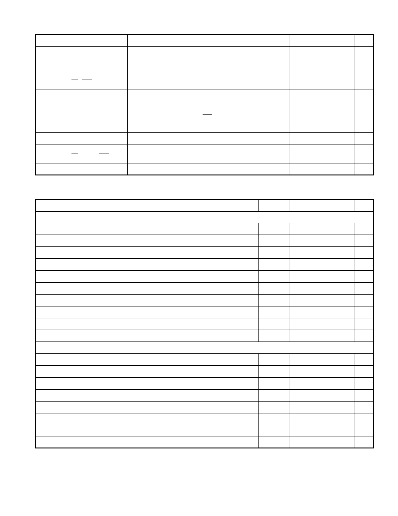
DC Electrical Characteristics: (VCC = 5V ±5%, VSS = 0, TA = 0° to +70°C unless otherwise specified)
Parameter
Symbol
Test Conditions
Min
Max Unit
Input High Voltage
Input Low Voltage
Input Current
(An, R/W, CSn)
Output High Voltage
Output Low Voltage
Output Leakage Current
(Three–State)
Supply Current
Input Capacitance
(An, R/W, CSn, CSn)
Output Capacitance (Dn)
VIH
VIL
Iin Vin = 0 to 5.25V
VSS +2.0 VCC
V
VSS –0.3 VSS +0.8 V
–
2.5 µA
VOH IOH = –205µA
VOL IOL = 1.6mA
ITSI CS = 0.8V or CS = 2V,
Vout = 0.4V to 2.4V
ICC VCC = 5.25V, All other pins grounded
Cin Vin = 0, TA = +25°C, f = 1MHz
2.4
–
V
–
0.4
V
–
10 µA
–
80 mA
–
7.5 pF
Cout Vout = 0, TA = +25°C, f = 1MHz, CSO = 0
–
12.5 pF
AC Operating Conditions and Characteristics:
Parameter
Symbol Min
Read Cycle (VCC = 5V ±5%, VSS = 0, TA = 0° to +70° unless otherwise specified)
Read Cycle Time
tcyc(R)
450
Access Time
tacc
–
Address Setup Time
tAS
20
Address Hold Time
tAH
0
Data Delay Time (Read)
tDDR
–
Read to Select Delay Time
tRCS
0
Data Hold from Address
tDHA
10
Output Hold Time
tH
10
Data Hold from Read
tDHR
10
Read Hold from Chip Select
tRH
0
Write Cycle (VCC = 5V ±5%, VSS = 0, TA = 0° to +70° unless otherwise specified)
Write Cycle Time
tcyc(W)
450
Address Setup Time
tAS
20
Address Hold Time
tAH
0
Chip Select Pulse Width
tCS
300
Write to Chip Select Delay Time
tWCS
0
Data Setup Time (Write)
tDSW
190
Input Hold Time
tH
10
Write Hold Time from Chip Select
tWH
0
Max Unit
–
ns
450 ns
–
ns
–
ns
230 ns
–
ns
–
ns
–
ns
80 ns
–
ns
–
ns
–
ns
–
ns
–
ns
–
ns
–
ns
–
ns
–
ns
Share Link: 