NTE2054 データシートの表示(PDF) - NTE Electronics
部品番号
コンポーネント説明
メーカー
NTE2054 Datasheet PDF : 3 Pages
| |||
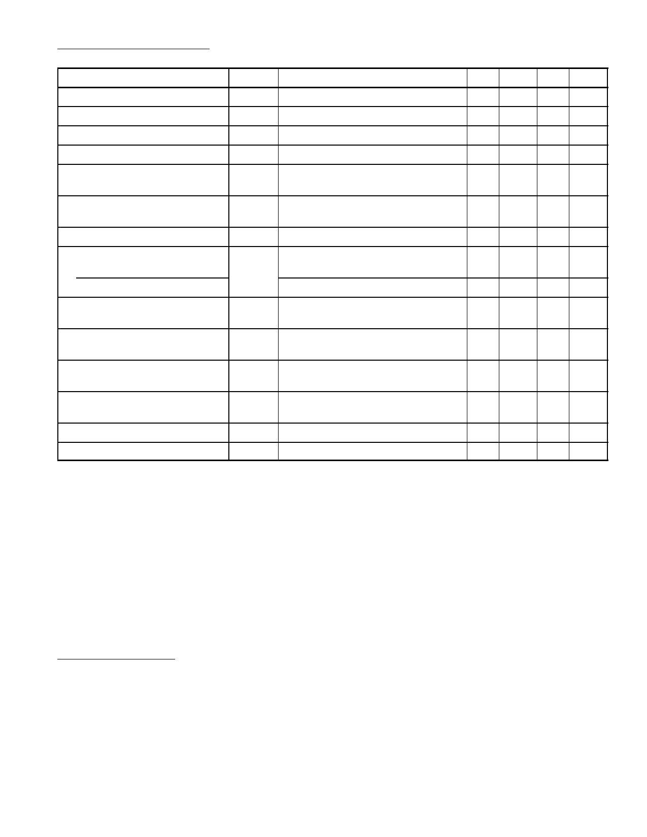
Electrical Characteristics: (TA = +25°C, V+ = 5V, Zero pot centered, gain pot = 2.4kΩ unless
otherwise specified)
Parameter
Symbol
Test Conditions
Min Typ Max Unit
Operating Supply Voltage Range V+
4.5 5.0 5.5 V
Supply Current
I+ 100kΩ to V+ on Pin3, Pin4, Pin5
– – 17 mA
Input Impedance
Input Bias Current
Unadjusted Zero Offset
Zi
IIB Pin10 and Pin11
V11 –V10 = 0V,
Read Decoded Output
– 100 – MΩ
– –80 – nA
–12 – +12 mV
Unadjusted Gain
V11 –V10 = 900mV,
Read Decoded Output
846 – 954 mV
Linearity
Note 1, Note 2
–1 – +1 Count
Conversion Rate
Slow Mode
Pin6 = Open or GND
– 4 – Hz
Fast Mode
Pin6 = 5V
– 96 – Hz
Conversion Control Voltage
(Hold Mode) at Pin6
0.8 1.2 1.6 V
Common–Mode Input
Voltage Range
VICR Note 3, Note 4
–0.2 – +0.2 V
BCD Sink Current at
Pin1, Pin2, Pin15, and Pin16
VBCD ≥ 0.5V, at Logic Zero State
0.4 1.6 – mA
Digit Select Sink Current at
Pin3, Pin4, and Pin5
VDigit Select = 4V at Logic Zero State 1.6 2.5 – mA
Zero Temperature Coefficient
Gain Temperature Coefficient
VI = 0V, Zero Pot Centered
VI = 900mV, Gain Pot = 2.4kΩ
– 10 – µV/°V
– 0.005 – %/°C
Note 1. Apply zero volts across V11 to V10. Adjust zero potentiometer to give 000mV reading. Apply
900mV to input and adjust gain potentiometer to give 900mV reading.
Note 2. Linearity is measured as a difference from a straight line drawn through zero and positive
full scale. Limits do not include ±0.5 count bit digitizing error.
Note 3. For applications where negative Pin10 is not operated at Pin7 potential, a return path of not
more than 100kΩ resistance must be provided for input bias currents.
Note 4. The common–mode input voltage above ground cannot exceed +0.2V if the full input signal
range of 999mV is required at Pin11. That is, Pin11 may not operate higher than 1.2V posi-
tive with respect to GND or 0.2V negative with respect to GND. If the maximum input signal
is less than 999mV, the common–mode input voltage may be raised accordingly.
Circuit Description:
The heart of the NTE2054 is the V/I converter and reference–current generator. The V/I converter
converts the input voltage applied between Pin10 and Pin11 to a current that charges the integrating
capacitor on Pin12 for a predetermined time interval. At the end of the charging interval, the V/I con-
verter is disconnected from the integrated capacitor, and a band–gap reference constant–current
source of opposite polarity is connected. The number of clock counts that elapse before the charge
is restored to its original value is a direct measure of the signal induced current. The restoration is
sensed by the comparator, which in turn latches the counter. The count is then multiplexed to the BCD
outputs.
Share Link: 